MC141555 View Datasheet(PDF) - Motorola => Freescale
Part Name
Description
Manufacturer
MC141555 Datasheet PDF : 16 Pages
| |||
Freescale Semiconductor, Inc.
ABSOLUTE MAXIMUM RATINGS Voltage Referenced to VSS
Symbol
Characteristic
Value
Unit
VDD
Supply Voltage
- 0.3 to + 7.0
V
Vin
Input Voltage
VSS – 0.3 to
V
VDD + 0.3
Id
Current Drain per Pin Excluding VDD and VSS
25
mA
Ta
Operating Temperature Range
Tstg
Storage Temperature Range
0 to 85
°C
– 65 to + 150
°C
NOTE: Maximum Ratings are those values beyond which damage to the device may occur.
Functional operation should be restricted to the limits in the Electrical Characteristics
tables or Pin Description section.
This device contains protection circuitry to guard
against damage due to high static voltages or
electric fields. However, precautions must be
taken to avoid applications of any voltage higher
than maximum rated voltages to this high-imped-
ance circuit. For proper operation, Vin and Vout
should be constrained to the range VSS ≤ (Vin
or Vout) ≤ VDD.
Unused inputs must always be tied to an appro-
priate logic voltage level (e.g., either VSS or
VDD). Unused outputs must be left open.
AC ELECTRICAL CHARACTERISTICS (VDD/VDD(A) = 5.0 V, VSS/VSS(A) = 0 V, TA = 25C,
Voltage Referenced to VSS)
FULL SPEED MODE CHARACTERISTICS
Symbol
Parameter
tr
Rise Time for DP/DM
tf
Fall Time for DP/DM
tRFM
Rise/Fall Time Matching
VCRS
Output Signal Crossover Voltage
Conditions
Min
Cload = 50 pF
4
Cload = 50 pF
4
(tr/tf) x 100
90
—
1.3
LOW SPEED MODE CHARACTERISTICS
Symbol
Parameter
tr
Rise Time for DP/DM
tf
Fall Time for DP/DM
tRFM
Rise/Fall Time Matching
VCRS
Output Signal Crossover Voltage
Conditions
Min
Cload = 50 pF to 350 pF
75
Cload = 50 pF to 350 pF
75
(tr/tf) x 100
80
—
1.3
Max
Unit
20
ns
20
ns
110
%
2.0
V
Max
Unit
300
ns
300
ns
120
%
2.0
V
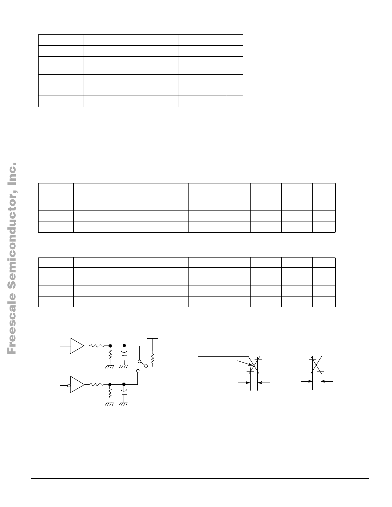
Data
R1
R2 Cload
R3
R1
DM
R2 Cload
R1 = 22 Ω
R2 = 15 kΩ
R3 = 1.5kΩ
Figure 2. Differential Driver Switching Load
DP
VCRS
90%
DM
10%
tr
90%
VOH
10% VOL
tf
Figure 3. Differential Driver Switching Characteristics
MOTOROLA
For More Information On This Product,
Go to: www.freescale.com
MC141555
3
Share Link: 