MC141563 View Datasheet(PDF) - Motorola => Freescale
Part Name
Description
Manufacturer
MC141563 Datasheet PDF : 15 Pages
| |||
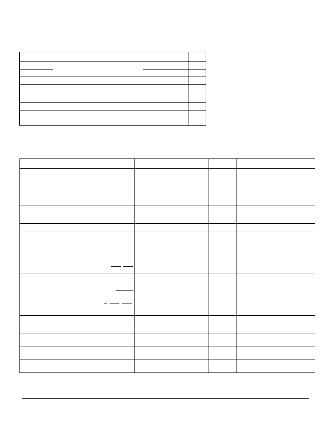
MAXIMUM RATINGS*(Voltages Referenced to VSS, TA=25C)
Symbol
Parameter
Value
Unit
VDD
Supply Voltage
-0.3 to +6.0
V
VEE
-0.3 to -24.0
V
VLCD
DC Supply Voltage (VDD - VEE)
VDD to +30
V
Input Voltage
VDin
All Digital Input
VAin
VLCD Level Input
VSS-0.3 to VDD+0.3
V
VEE-0.3 to VDD+0.3
V
I
Current Drain Per Pin Excluding VDD and VSS
25
mA
TA
Operating Temperature Range
-20 to 70
˚C
Tstg
Storage Temperature Range
-65 to +150
˚C
* Maximum Ratings are those values beyond which damage to the device may occur. Functional
operation should be restricted to the limits in the Electrical Characteristics tables or Pin Description
section.
This device contains circuitry to protect the inputs
against damage due to high static voltages or elec-
tric fields; however, it is advised that normal precau-
tions to be taken to avoid application of any voltage
higher than maximum rated voltages to this high
impedance circuit. For proper operation it is recom-
mended that Vin and Vout be constrained to the
range VSS < or = (Vin or Vout) < or = VDD. Reliability
of operation is enhanced if unused input are con-
nected to an appropriate logic voltage level (e.g.,
either VSS or VDD). Unused outputs must be left
open. This device may be light sensitive. Caution
should be taken to avoid exposure of this device to
any light source during normal operation. This
device is not radiation protected.
ELECTRICAL CHARACTERISTICS (Voltage Referenced to VSS, TA = 25˚C)
Symbol
Parameter
Test Condition
Min
Typ
Max
Unit
VDD
VLCD
IDP
ISB
IDP
ISB
IEE
VOL
VOH
Operating Voltage
Supply Voltage (reference to VSS)
LCD Supply Voltage ( VDD - VEE)
Supply Current (VDD Pin)
Display Mode
Standby Mode
VDD=5.5V, VEE=-23V
SCLK = 6MHz, LP=15KHz,
M=35Hz
Supply Current (VDD Pin)
Display Mode
Standby Mode
VDD=2.7V, VEE=-23V
SCLK = 6MHz, LP=15KHz,
M=35Hz
Supply Current at VEE
Segment Output Voltage
VL4,6=VEE
VL1,3=VDD
No Load
Iload = 100A
SEG1-SEG80
V
2.7
-
5.5
V
10.0
-
28.0
-
250
600
A
-
1.5
5.5
A
-
120
-
A
-
600
-
nA
-
30
550
A
-
-
VEE+0.3
V
VDD-0.3
-
-
V
VOH
Output High Voltage
VOL
Output Low Voltage
VDD=5.0V, Iload=1mA
EIO1, EIO2
VDD-1.0
-
-
V
-
-
VSS+1.0
V
VIH
Input High Voltage
VIL
Input Low Voltage
SCLK, LP, L/R, EIO1, EIO2,
D0 to D3, M, DIS-OFF
0.7xVDD
-
VDD
V
VSS
-
0.2xVDD
V
Iin
Input Current
SCLK, LP, L/R, EIO1, EIO2,
D0 to D3, M, DIS-OFF
-
0.5
1.0
A
Cin
Capacitance
SCLK, LP, L/R, EIO1, EIO2,
D0 to D3, M, DIS-OFF
-
5
10
pF
IOHX, IOLX Segment Output Current
VOH= VDD - 0.3V, VOL=VEE +0.3V
100
-
SEG1-SEG80
-
A
IOHC, IOLC Carry Output Current
VOH= VDD - 1.0V, VOL=VSS +1.0V
1.0
-
EIO1, EIO2
-
mA
RON
Segment Output Impedance
VDD - VEE =28V, IOHX, IOLX=100A
-
Segment Output Impedance Variance
-
1.5
3.0
K Ohm
10
30
%
MOTOROLA
MC141563
3–323
Share Link: 