MC141563 View Datasheet(PDF) - Motorola => Freescale
Part Name
Description
Manufacturer
MC141563 Datasheet PDF : 15 Pages
| |||
PIN DESCRIPTIONS
VDD AND VSS
The main dc power is supplied to the part by these two connections.
VDD is the most-positive supply level and VSS is ground.
VEE
This supply connection provides the negative power supply voltage
for the common drivers.
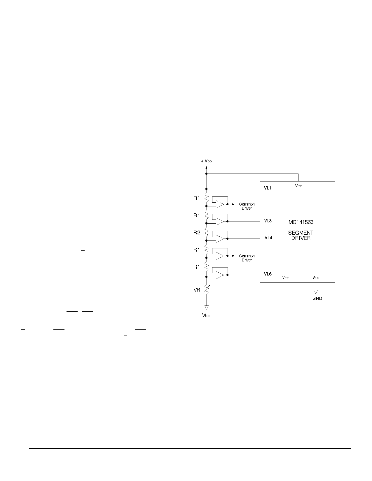
VL1, VL3, VL4, VL6
These input pins are connected to the external voltage divider (See
Figure 8).
Voltage supply level for the LCD :
VL1, VL6 : On-level of the LC
VL3, VL4 : Off-level of the LC
Data Latch (LP)
Display data (a complete line on display) is acknowledged by the
falling edge of the LP signal.
Data Shift Clock (SCLK)
Input data (8 bit or 4 bit) is stored into a 8 bit / 4 bit data latch by the
falling edge of SCLK.
Data Input (D0 to D7)
Data Input is either in 8 bit or 4 bit data bus format and is select-
able by the DS input.
Data Format Select (DS)
This input is to select the data bus format. If set “Low”, the data bus
format is 4-bit, if set “High”, the data bus format is 8-bit.
Left / Right Shift Select (L / R)
This input pin provides the selection of the shift register operation
(See Table 1).
L / R = “1”,
the data will shift left
(LSB of the first input data will be
loaded to SEG1).
L / R = “0”,
the data will shift right
(LSB of the first input data will be
loaded to SEG80).
Carry-In / Carry-Out (EIO1 / EIO2)
These two input / output pins perform the same function and
depend on the shift register direction of operation. In right shift mode (L
/ R = “0”), the EIO1 is the Carry-In input while the EIO2 will be the
Carry-Out output for cascading. In Left Mode (L / R = “1”), the pin func-
tions and operation are reversed. (See Table 2)
Frame Signal Input (M)
This input signal is the frame sync. signal which provides an frame
alternating output format of the segment output (See Figure 9).
M
Data
Output
0
0
1
1
1
0
0
1
VL1 VL3 VL4 VL6
Display-Off Enable (DIS-OFF)
This input pin is active low. If set “LOW”, all output pins (Segment 1
to Segment 80) are forced to VL1.
Segment Output (Segment 1 to Segment 80)
These 80 output lines provide the high volt segment signal to the
LCD panel. They are all at VL1 while display is turned off.
Figure 8. External Voltage Divider
MC141563
3–326
MOTOROLA
Share Link: 