MC33151VDR2G View Datasheet(PDF) - ON Semiconductor
Part Name
Description
Manufacturer
MC33151VDR2G Datasheet PDF : 12 Pages
| |||
MC34151, MC33151
90%
VCC = 12 V
Logic Input
Vin = 5 V to 0 V
CL = 1.0 nF
TA = 25°C
10%
Drive Output
50 ns/DIV
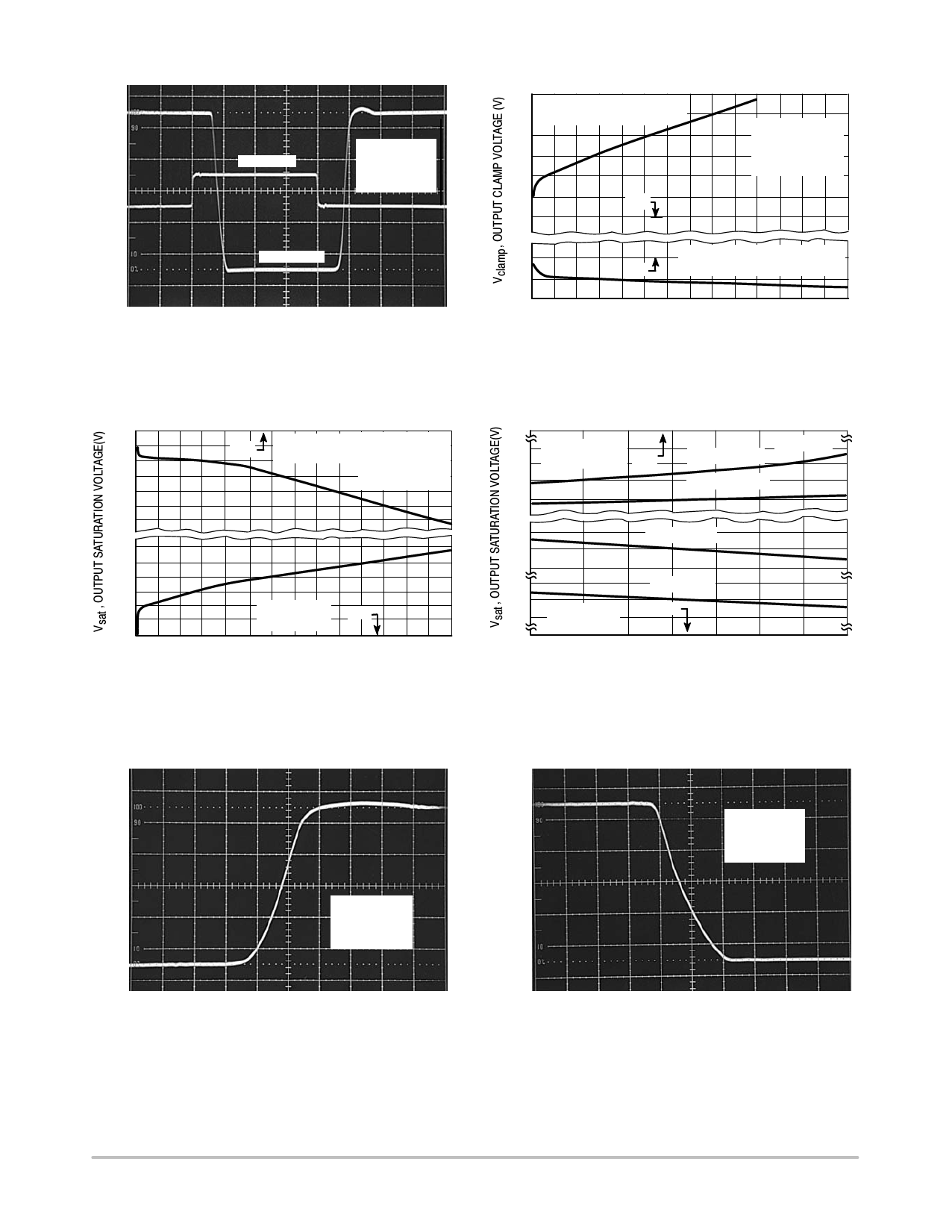
Figure 8. Propagation Delay
3.0
High State Clamp
(Drive Output Driven Above VCC)
2.0
1.0
VCC
0
VCC = 12 V
80 ms Pulsed Load
120 Hz Rate
TA = 25°C
0
-1.0
0
Low State Clamp
GND
(Drive Output Driven Below Ground)
0.2
0.4
0.6
0.8
1.0
1.2
1.4
IO, OUTPUT LOAD CURRENT (A)
Figure 9. Drive Output Clamp Voltage
versus Clamp Current
0
-1.0
VCC
Source Saturation VCC = 12 V
(Load to Ground) 80 ms Pulsed Load
120 Hz Rate
-2.0
TA = 25°C
-3.0
3.0
2.0
1.0
Sink Saturation
(Load to VCC)
GND
0
0
0.2
0.4
0.6
0.8
1.0
1.2
1.4
IO, OUTPUT LOAD CURRENT (A)
Figure 10. Drive Output Saturation Voltage
versus Load Current
0
-0.5
-0.7
Source Saturation
(Load to Ground) VCC
-0.9
-1.1
VCC = 12 V
Isource = 10 mA
Isource = 400 mA
1.9
Isink = 400 mA
1.7
1.5
1.0
Isink = 10 mA
0.8
0.6
Sink Saturation
(Load to VCC)
GND
0
-55
-25
0
25
50 75
TA, AMBIENT TEMPERATURE (°C)
100 125
Figure 11. Drive Output Saturation Voltage
versus Temperature
90%
VCC = 12 V
Vin = 5 V to 0 V
CL = 1.0 nF
10%
TA = 25°C
10 ns/DIV
Figure 12. Drive Output Rise Time
90%
VCC = 12 V
Vin = 5 V to 0 V
CL = 1.0 nF
TA = 25°C
10%
10 ns/DIV
Figure 13. Drive Output Fall Time
http://onsemi.com
5
Share Link: 