MC33411A View Datasheet(PDF) - Motorola => Freescale
Part Name
Description
Manufacturer
MC33411A Datasheet PDF : 43 Pages
| |||
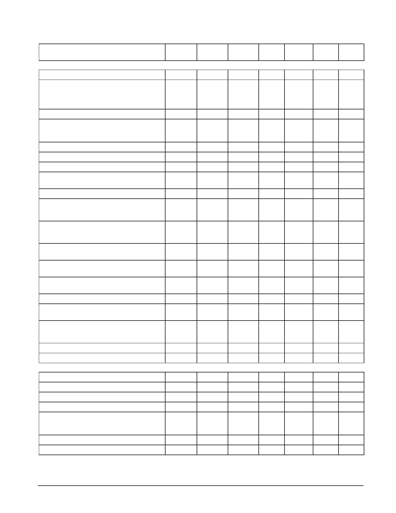
MC33411A/B
ELECTRICAL CHARACTERISTICS (continued) (VCC = 3.6 V, VB = 1.5 V, TA = 25°C, Active Mode, Rx Gain = 01111,
Vol Adj = 0111, fin = 1.0 kHz, unless otherwise noted.)
Characteristics
Input
Measure
Pin
Pin
Symbol
Min
Typ
Max
Tx AUDIO PATH (VCC = 3.6 V, Limiter, Mutes, ALC disabled, TA = 25°C, Gain = 1, Active Mode, fin = 1.0 kHz)
Absolute Gain (Vin = –10 dBV)
MCI
TX Out
G
–4.0
0
4.0
Gain Tracking (Referenced to Tx Out for
Vin = –10 dBV)
Vin = –30 dBV
Vin = –40 dBV
Total Harmonic Distortion (Vin = –10 dBV)
MCI
Tx Out
Gt
–11
–10
–9.0
–17
–15
–13
MCI
Tx Out
THD
–
0.5
1.2
Maximum Output Voltage (Increase input voltage
MCI
Tx Out
VOmax
–8.0
–5.0
–
until output voltage THD = 5%, then measure
output voltage. Tx Gain Adj = 8.0 dB)
Input Impedance
Attack Time Ccap = 0.5 µF, Rfilt = 40 k
C In
Release Time Ccap = 0.5 µF, Rfilt = 40 k
C In
Expander to Compressor Crosstalk (Vin = –20 dBV,
E In
PA no load, VCin = AC Gnd)
Tx Muting (Vin = –10 dBV)
MCI
ALC Output Level (When Enabled)
MCI
Vin = –10 dBV
Vin = –2.5 dBV
ALC Slope (When Enabled)
MCI
Vin = –10 dBV
Vin = –2.5 dBV
ALC Input Dynamic Range
C In
C In
Zin
Tx Out
ta
Tx Out
tr
Tx Out
CT
–
10
–
–
3.0
–
–
13.5
–
–
–60
–40
Tx Out
Mc
–
–88
–60
Tx Out
ALCout
–15
–13
–8.0
–13
–11
–6.0
Tx Out
Slope
0.1
0.25
0.4
Tx Out
DR
–
–16 to
–
–2.5
Limiter Output Level (When Enabled, Vin = –2.5
Lim In
Tx Out
Vlim
–10
–7.0
–
dBV)
Tx High Frequency Corner (Vin = –10 dBV,
Unity Gain) SCF Counter = 31d
Lim In
Tx Out
Tx fch
3.45
3.65
3.85
Low Pass Filter Passband Ripple (Vin = –10 dBV)
Lim In
Tx Out
Ripple
–
0.4
1.0
MCU Clock or SCF Spurs (Vin = –10 dBv, relative to Lim In
Tx Out
–
SCF or MCU Fundamental)
–
–25
–
Maximum Compressor Gain (Vin = –70 dBV)
R6/8 = 0
R6/8 = 1
Tx Gain Adjust Range
MCI
Lim In
Tx Out
AVmax
Tx Out Tx Range
–
21
–
–
12
–
–
–9.0 to 10
–
Tx Gain Adjust Steps
Lim In
Tx Out
Tx N
–
20
–
DATA AMP COMPARATOR (VCC = 3.6 V, VB = 1.5 V, TA = 25°C, Active or Receive Mode)
Hysteresis
DS In
DS Out
Hys
20
42
60
Threshold Voltage
Input Impedance
Output Impedance
Output High Voltage (Vin = VCC – 1.0 V, Ioh = 0 mA)
DS In
DS In
DS Out
DS In
DS Out
DS Out
VT
Zin
Zout
Voh
–
VCC – 0.7
–
200
250
280
–
100
–
VCC
VCC
–
Audio
Audio
– 0.1
Output Low Voltage (Vin = VCC – 0.4 V, Iol = 0 mA)
DS In
DS Out
Vol
–
Maximum Frequency
DS In
DS Out
Fmax
–
NOTES: 1. Values specified are pure numbers to the base 10.
2. Typical performance parameters indicate the potential of the device under ideal operating conditions.
0.1
0.4
10
–
Unit
dB
dB
%
dBV
kΩ
mS
mS
dB
dB
dBV
dB/dB
dBV
dBV
kHz
dB
dBc
dB
dB
mV
V
kΩ
kΩ
V
V
kHz
MOTOROLA RF/IF DEVICE DATA
5
Share Link: 