MC34055DW View Datasheet(PDF) - Motorola => Freescale
Part Name
Description
Manufacturer
MC34055DW Datasheet PDF : 16 Pages
| |||
MC34055
The figures show the voltage waveforms on the differential
driver output pins. To actually meet the 10BASE–T
specification requires bandpass filtering and a pulse
transformer.
The output voltage waveform specifications of the IEEE
802.3 standard require that voltages impressed on the
twisted pair meet a voltage template. The MC34055 can
meet the voltage template for all the 10BASE–T applications
initiated. In this event, the transmit differential driver will
remain active for the entire frame interval and the link pulse
will not affect more than one bit interval.
The MC34055 also has Jabber circuitry to detect and
disable the twisted pair driver in the event that a serial
controller fails constantly transmitting. Should any data
source try to transmit longer than 20 ms minimum, the Jabber
function will disable the differential driver outputs, the
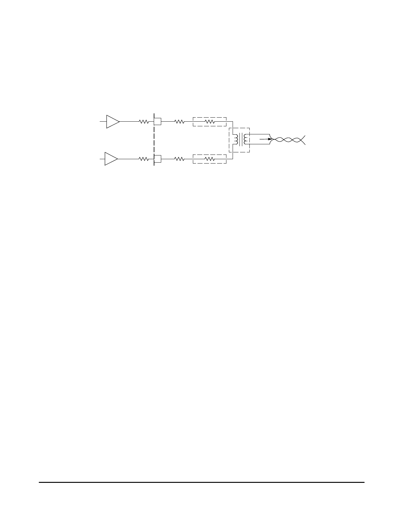
Figure 8. Differential Driver Media Interface Circuitry
+1
TX+
20
ZOD/2
RS
Pulse
Transformer
ZF
Twisted Pair
ZO
–1
ZOD/2 21 TX– RS
ZF
Where: ZOD is the transmitters differential output impedance (~20 Ω),
Where: RS is a 1% series resistor,
Where: ZF is the filters impedance, and ZO is the characteristic
Where: impedance of the twisted pair (100 Ω).
by choosing the appropriate low pass filter and external
components in the driver output circuitry. When the
differential transmit driver output pins are configured to drive
the bandpass filters and pulse transformer as shown in
Figure 8, the resultant waveform is capable of meeting the
voltage template.
Following the end–of–frame activity, an internal pull–up
resistor pulls TX Data A/B high and causes the differential
driver to maintain full differential output voltage for
approximately 250 ns. The differential driver interprets the
lack of transition activity as an end of frame and starts an idle
timer. Should another frame intended for the twisted pair
arrive before the idle timer expires(~250 ns), the idle timer
will be reset, if not, the transmit driver function will begin the
decay to idle process. During idle periods the differential
driver must force the media to a minimal differential voltage
unless a link beat is being produced. The transition to
minimal voltage is subject to performance requirements in
the IEEE specification and is met by the MC34055 when the
appropriate filters and transformers are used to interface to
the media.
The MC34055 differential driver generates link pulses
(beats) during idle periods. The link pulses produced are
singular positive (TX+ positive with respect to TX–) pulses
applied to the media at 16 ms intervals and last
approximately 100 ns. The link pulses allow the receiver at
the other end of the link to verify the validity of the segment.
There is the possibility, due to the two asynchronous
sources, that one of the two input pins (TX Data A or TX Data
B) will receive frame activity immediately after a link pulse is
collision presence detector and the internal loopback
function. Also, two status indicator pins, CTL H and JABB H
are asserted. The MC34055 will remain in the jabber state
until the TX EN H pin is pulled low or the jabbering input
ceases to toggle for a minimum of 500 ms. The status
indicator pins, CTL H and JABB H will also sink up to 20 mA
and can therefore support external LEDs.
The driver also works with the receiver to provide
loop–back. Under normal operating conditions (Loop L= “1”),
the data applied to the TX Data A/B pins is looped back
internally to the RX Data A/B pins. This function is disabled
when there is a collision condition or FULLD L is low.
Data Reception
Data intended for the DTE proceeds from the twisted pair
to the isolation transformer and bandpass filters before
reaching the differential receiver terminals. Figure 9 shows
the configuration of the external media receive circuitry. Once
transitions at the receiver terminals (RX+ and RX–) are
detected, the on–chip oscillator is synchronized and the
received data is screened by smart squelch circuitry for
validity. This qualification requires incoming data to meet
amplitude and sequence requirements. If the data meets the
Smart Squelch requirements, the receiver enters the
unsquelch state and the data is forwarded to the RX Data A/B
output pins provided Loop L is not low. Two data outputs are
provided to increase design flexibility, RX Data A and RX
Data B. RX Data A is CMOS/TTL compatible and RX Data B
is raised ECL compatible.
MOTOROLA ANALOG IC DEVICE DATA
9
Share Link: 