MC33880DW View Datasheet(PDF) - Motorola => Freescale
Part Name
Description
Manufacturer
MC33880DW Datasheet PDF : 24 Pages
| |||
Freescale Semiconductor, Inc.
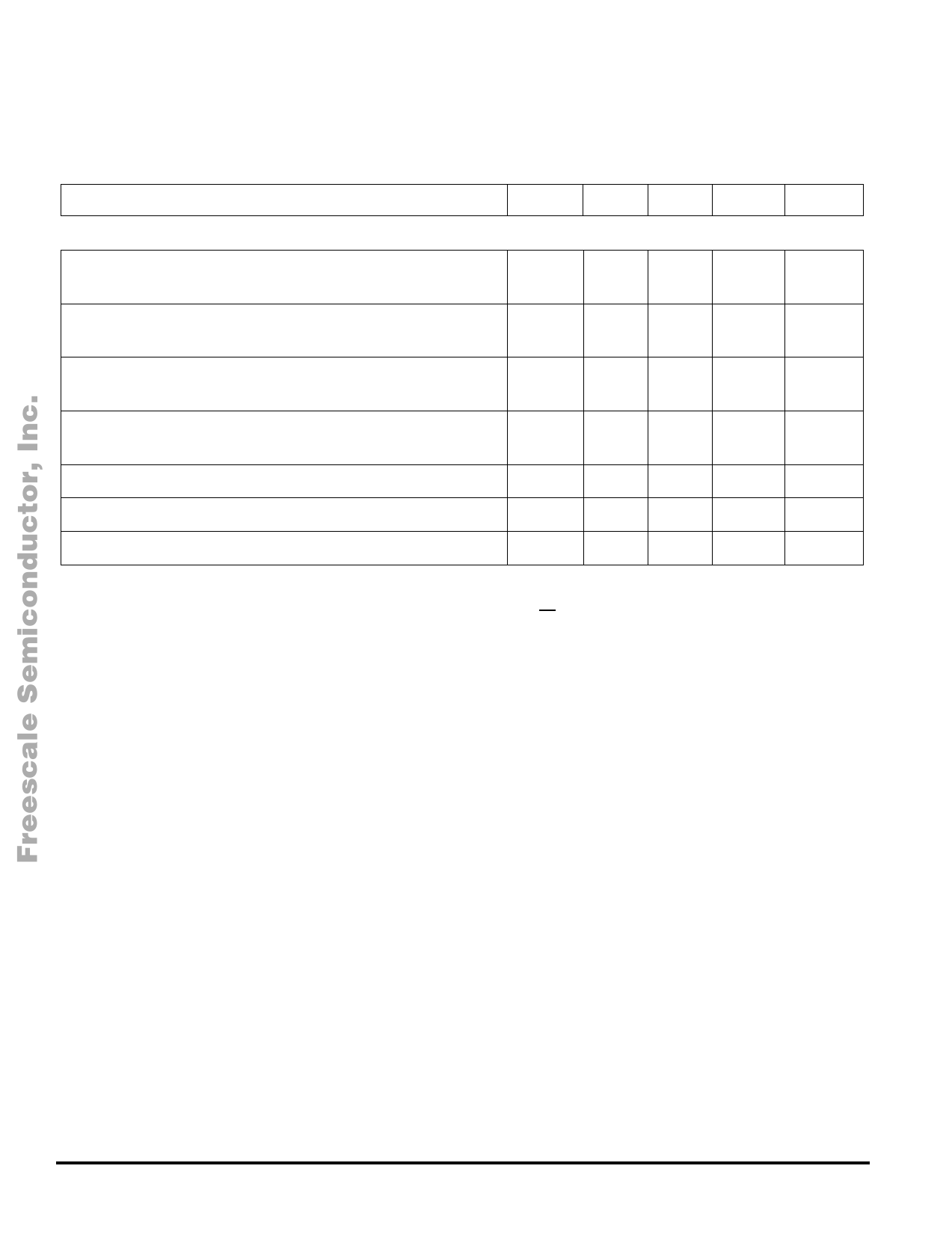
DYNAMIC ELECTRICAL CHARACTERISTICS
Characteristics noted under conditions of 4.75 V ≤ VDD ≤ 5.25 V, 9.0 V ≤ VPWR ≤ 16 V, -40°C ≤ TC ≤ 125°C unless otherwise
noted. Typical values, where applicable, reflect the parameter’s approximate average value with VPWR = 13 V, TA = 25°C.
Characteristic
Symbol
Min
Typ
Max
Units
POWER OUTPUT TIMING
Output Slew Rate Low-Side Configuration (Note 13)
RL = 620 Ω
tR
0.1
0.5
1.2
Output Slew Rate Low-Side Configuration (Note 13)
RL = 620 Ω
tF
0.1
0.5
1.2
Output Slew Rate High-Side Configuration (Note 13)
RL = 620 Ω
tR
0.1
0.3
1.2
Output Slew Rate High-Side Configuration (Note 13)
RL = 620 Ω
tF
0.1
0.3
1.2
Output Turn ON Delay Time, High-Side and Low-Side Configuration (Note 14) tDLY(ON)
1.0
15
50
Output Turn OFF Delay Time, High-Side and Low-Side Configuration (Note 14) tDLY(OFF)
1.0
30
100
Output Fault Delay Time (Note 15)
tFAULT
100
–
300
V/µs
V/µs
V/µs
V/µs
µs
µs
µs
Notes:
13. Output Rise and Fall time respectively measured across a 620 Ω resistive load at 10 to 90 percent and 90 to 10 percent voltage points.
14. Output turn ON and OFF delay time measured from 50 percent rising edge of CS to 90 and 10 percent of initial voltage.
15. Duration of fault before fault bit is set. Duration between access times must be greater than 300 µs to read faults.
33880
10
For More Information OMnOTTOhRiOsLAPrAoNdAuLOcGt,INTEGRATED CIRCUIT DEVICE DATA
Go to: www.freescale.com
Share Link: 