AM6012D View Datasheet(PDF) - Philips Electronics
Part Name
Description
Manufacturer
AM6012D Datasheet PDF : 11 Pages
| |||
Philips Semiconductors Linear Products
12-Bit multiplying D/A converter
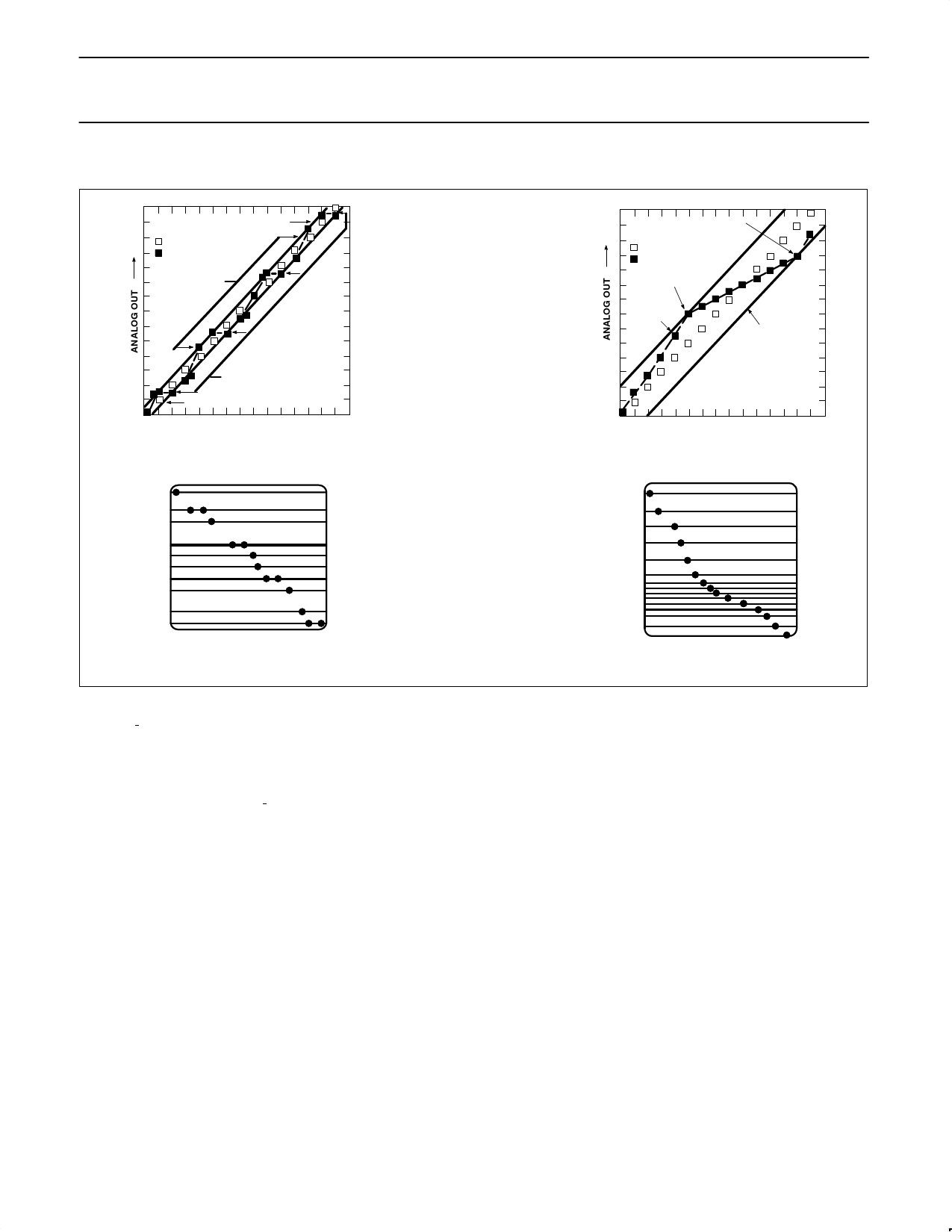
DIFFERENTIAL LINEARITY COMPARISON
+1/2LSB
LIMIT
IDEAL OUTPUTS
ACUTAL OUTPUTS
2LSB CHANGE ON
X011–X100
TRANSITION
SEGMENT
OF 12-BIT
DAC TRANSFER
CURVE FOR:
INL = ±1/2LSB
DNL = ±1LSB
NO CHANGE ON
XX01–XX10 TRANSITION
–1/2LSB LIMIT
0000 0010 0100 0110 1000 1010 1100 1110
0001 0011 0101 0111 1001 1011 1101 1111
DIGITAL INPUT
±1/2LSB INL, ±1LSB DNL
Product specification
AM6012
SEGMENT
CHANGE
IDEAL OUTPUTS
ACUTAL OUTPUTS
SEGMENT
CHANGE
+2LSB
LIMIT
–2 LSB
LIMIT
SEGMENT OF 12-BIT DAC
TRANSFER CURVE FOR:
INL = ±2LSB
DNL = ±ℑ√2LSB
0010 0010 0100 0110 1000 1010 1100 1110
0001 0011 0101 0111 1001 1011 1101 1111
DIGITAL INPUT
±2LSB INL, ±1LSB DNL
Figure 1. Differential Linearity Comparison
ANALOG OUTPUT CURRENTS
Both true and complemented output sink currents are provided
where IO+IO=IFR. Current appears at the “true” output when a “1” is
applied to each logic input. As the binary count increases, the sink
current at Pin 18 increases proportionally, in the fashion of a
“positive logic” D/A converter. When a “0” is applied to any input bit,
that current is turned off at Pin 18 and turned on at Pin 19. A
decreasing logic count increases IO as in a negative or inverted logic
D/A converter. Both outputs may be used simultaneously. If one of
the outputs is not required, it must still be connected to ground or to
a point capable of sourcing IFR; do not leave an unused output pin
open.
Both outputs have an extremely wide voltage compliance enabling
fast direct current-to-voltage conversion through a resistor tied to
ground or other voltage source. Positive compliance is 25V above V-
and is independent of the positive supply. Negative compliance is
+10V above V-.
The dual outputs enable double the usual peak-to-peak load swing
when driving loads in quasi-differential fashion. This feature is
especially useful in cable driving, CRT deflection and in other
balanced applications such as driving center-tapped coils and
transformers.
compliance, reference amplifier negative common-mode range,
negative logic input range, and negative logic threshold range;
consult the various figures for guidance. For example, operation at
-9V with IREF=1mA is not recommended because negative output
compliance would be reduced to near zero. Operation from lower
supplies is possible, however at least 8V total must be applied to
insure turn-on of the internal bias network.
Symmetrical supplies are not required, as the AM6012 is quite
insensitive to variations in supply voltage. Battery operation is
feasible as no ground connection is required; however, an artificial
ground may be used to insure logic swings, etc., remain between
acceptable limits.
TEMPERATURE PERFORMANCE
The nonlinearity and monotonicity specifications of the AM6012 are
guaranteed to apply over the entire rated operating temperature
range. Full-scale output current drift is tight, typically ±10ppm/°C,
with zero-scale output current and drift essentially negligible
compared to 1/2LSB.
The temperature coefficient of the reference resistor R14 should
match and track that of the output resistor for minimum overall
full-scale drift.
POWER SUPPLIES
The AM6012 operates over a wide range of power supply voltages
from a total supply of 20V to 36V. When operating with V- supplies
of -10V or less, IREF≤1mA is recommended. Low reference current
operation decreases power consumption and increases negative
SETTLING TIME
The AM6012 is capable of extremely fast settling times, typically
250ns at IREF=1.0mA. Judicious circuit design and careful board
layout must be employed to obtain full performance potential during
August 31, 1994
780
Share Link: 