MCH3474(2009) View Datasheet(PDF) - SANYO -> Panasonic
Part Name
Description
Manufacturer
MCH3474 Datasheet PDF : 4 Pages
| |||
MCH3474
Continued from preceding page.
Parameter
Symbol
Static Drain-to-Source On-State Resistance
Input Capacitance
Output Capacitance
Reverse Transfer Capacitance
Turn-ON Delay Time
Rise Time
Turn-OFF Delay Time
Fall Time
Total Gate Charge
Gate-to-Source Charge
Gate-to-Drain “Miller” Charge
Diode Forward Voltage
RDS(on)1
RDS(on)2
RDS(on)3
Ciss
Coss
Crss
td(on)
tr
td(off)
tf
Qg
Qgs
Qgd
VSD
Conditions
ID=2A, VGS=4.5V
ID=1A, VGS=2.5V
ID=0.5A, VGS=1.8V
VDS=10V, f=1MHz
VDS=10V, f=1MHz
VDS=10V, f=1MHz
See specified Test Circuit.
See specified Test Circuit.
See specified Test Circuit.
See specified Test Circuit.
VDS=15V, VGS=4.5V, ID=4A
VDS=15V, VGS=4.5V, ID=4A
VDS=15V, VGS=4.5V, ID=4A
IS=4A, VGS=0V
Ratings
Unit
min
typ
max
38
50 mΩ
51
72 mΩ
80
130 mΩ
430
pF
59
pF
38
pF
10
ns
41
ns
36
ns
37
ns
4.7
nC
0.8
nC
1.1
nC
0.82
1.2
V
Package Dimensions
unit : mm (typ)
7019A-003
2.0
0.15
3
0 t o 0.02
1
2
0.65
0.3
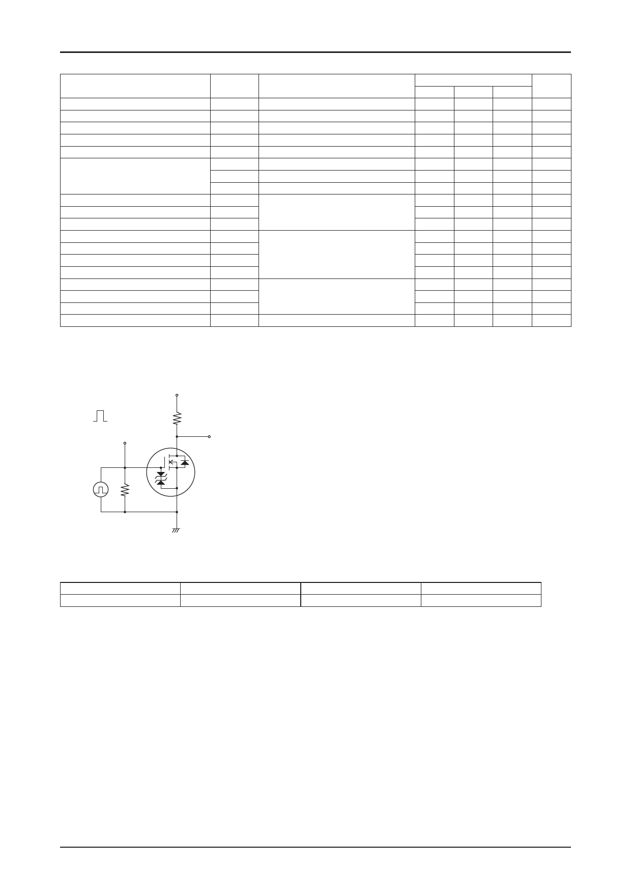
Switching Time Test Circuit
VIN
4.5V
0V
PW=10μs
D.C.≤1%
VIN
G
VDD=15V
ID=2A
RL=7.5Ω
D
VOUT
P.G
50Ω
S MCH3474
1 : Gate
2 : Source
3 : Drain
SANYO : MCPH3
ID -- VDS
4.0
3.5
3.0
2.5
2.0
1.5
1.5V
1.0
0.5
VGS=1.2V
0
0 0.1 0.2 0.3 0.4 0.5 0.6 0.7 0.8 0.9 1.0
Drain-to-Source Voltage, VDS -- V IT14344
ID -- VGS
5.0
VDS=10V
4.5
4.0
3.5
3.0
2.5
2.0
1.5
1.0
0.5
0
0 0.2 0.4 0.6 0.8 1.0 1.2 1.4 1.6 1.8 2.0
Gate-to-Source Voltage, VGS -- V IT14345
No. A1397-2/4
Share Link: 