MCM321024 View Datasheet(PDF) - Motorola => Freescale
Part Name
Description
Manufacturer
MCM321024 Datasheet PDF : 8 Pages
| |||
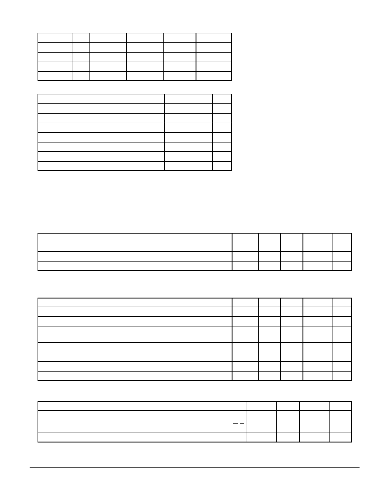
TRUTH TABLE
Ex G W
H
X
X
L
H
H
L
L
H
L
X
L
Mode
Not Selected
Read
Read
Write
VCC Current
ISB1 or ISB2
ICCA
ICCA
ICCA
Output
High–Z
High–Z
Dout
Din
Cycle
—
—
Read Cycle
Write Cycle
ABSOLUTE MAXIMUM RATINGS (Voltages referenced to VSS = 0 V)
Rating
Symbol
Value
Unit
Power Supply Voltage
VCC
– 0.5 to 7.0
V
Voltage Relative to VSS
Vin, Vout – 0.5 to VCC + 0.5 V
Output Current (per I/O)
Iout
± 30
mA
Power Dissipation
PD
8.0
W
Temperature Under Bias
Tbias
– 10 to + 85
°C
Operating Temperature
TA
0 to + 70
°C
Storage Temperatrue
Tstg
– 25 to + 125
°C
NOTE: Permanent device damage may occur if ABSOLUTE MAXIMUM RATINGS are ex-
ceeded. Functional operation should be restricted to RECOMMENDED OPERAT-
ING CONDITIONS. Exposure to higher than recommended voltages for extended
periods of time could affect device reliability.
The devices on this module contain circuitry
to protect the inputs against damage due to
high static voltages or electric fields; however,
it is advised that normal precautions be taken
to avoid application of any voltage higher than
maximum rated voltages to these high imped-
ance circuits.
These CMOS memory circuits have been
designed to meet the dc and ac specifications
shown in the tables, after thermal equilibrium
has been established. The module is in a test
socket or mounted on a printed circuit board
and transverse air flow of at least 500 linear
feet per minute is maintained.
DC OPERATING CONDITIONS AND CHARACTERISTICS
(VCC = 5.0 V ± 10%, TA = 0 to + 70°C, Unless Otherwise Noted)
RECOMMENDED OPERATING CONDITIONS (Voltages Referenced to VSS = 0 V)
Parameter
Symbol Min
Typ
Max
Unit
Supply Voltage (Operating Voltage Range)
VCC
4.5
5.0
5.5
V
Input High Voltage
VIH
2.2
— VCC + 0.3* V
Input Low Voltage
* VIH (max) = VCC + 0.3 V dc; VIH (max) = VCC + 2 V ac (pulse width ≤ 20 ns)
** VIL (min) = – 3.0 V ac (pulse width ≤ 20 ns)
VIL
– 0.5**
—
0.8
V
DC CHARACTERISTICS
Parameter
Symbol Min
Typ
Max
Unit
Input Leakage Current (All Inputs, Vin = 0 to VCC)
Ilkg(I)
—
—
±8
µA
Output Leakage Current (G, Ex = VIH, Vout = 0 to VCC)
Ilkg(O)
—
—
±8
µA
AC Active Supply Current (G, Ex = VIL, Iout = 0 mA, MCM321024–20: tAVAV = 20 ns ICCA
—
1440
1520
mA
Cycle time ≥ tAVAV min)
MCM321024–25: tAVAV = 25 ns
—
1320
1400
AC Standby Current (Ex = VIH, Cycle time ≥ tAVAV min)
ISB1
—
400
480
mA
CMOS Standby Current (Ex ≥ VCC – 0.2 V, All Inputs ≥ VCC – 0.2 V or ≤ 0.2 V)
ISB2
—
80
120
mA
Output Low Voltage (IOL = + 8.0 mA)
VOL
—
—
0.4
V
Output High Voltage (IOH = – 4.0 mA)
NOTE: Good decoupling of the local power supply should always be used.
VOH
2.4
—
—
V
CAPACITANCE (f = 1.0 MHz, dV = 3.0 V, TA = 25°C, Periodically Sampled Rather Than 100% Tested)
Characteristic
Symbol
Typ
Max
Unit
Input Capacitance
(All pins except DQ0 – DQ31, W, G, and E1 – E4)
Cin
32
48
pF
E1 – E4
10
14
W, G
40
64
Input/Output Capacitance
(DQ0 – DQ31) Cout
8
9
pF
MOTOROLA FAST SRAM
MCM321024
3
Share Link: 