MCM72F8 View Datasheet(PDF) - Motorola => Freescale
Part Name
Description
Manufacturer
MCM72F8 Datasheet PDF : 12 Pages
| |||
ABSOLUTE MAXIMUM RATINGS (Voltages Referenced to VSS = 0 V)
Rating
Symbol
Value
Unit
Power Supply Voltage
VDD
– 0.5 to + 4.6
V
Voltage Relative to VSS (See Note 2)
Vin, Vout – 0.5 to VDD + 0.5 V
Input Voltage Three State I/O (See Note 2)
VIT
– 0.5 to VDD + 0.5 V
Output Current (per I/O)
Iout
± 20
mA
Power Dissipation
MCM72F8 PD
MCM72F9
4.6
W
9.2
Ambient Temperature
TA
0 to 70
°C
Die Temperature
TJ
110
°C
Temperature Under Bias
Tbias
– 10 to + 85
°C
Storage Temperature
Tstg
– 55 to + 125
°C
NOTES:
1. Permanent device damage may occur if ABSOLUTE MAXIMUM RATINGS are
exceeded. Functional operation should be restricted to RECOMMENDED OPER-
ATING CONDITIONS. Exposure to higher than recommended voltages for extended
periods of time could affect device reliability.
2. This is a steady–state DC parameter that is in effect after the power supply has
achieved its nominal operating level. Power sequencing cannot be controlled and is
not allowed.
This device contains circuitry to protect the
inputs against damage due to high static volt-
ages or electric fields; however, it is advised that
normal precautions be taken to avoid application
of any voltage higher than maximum rated volt-
ages to this high–impedance circuit.
This BiCMOS memory circuit has been
designed to meet the dc and ac specifications
shown in the tables, after thermal equilibrium
has been established.
This device contains circuitry that will ensure
the output devices are in High–Z at power up.
DC OPERATING CONDITIONS AND CHARACTERISTICS
(VDD = 3.3 V + 10%, – 5%, TA = 0 to 70°C, Unless Otherwise Noted)
RECOMMENDED OPERATING CONDITIONS (Voltages Referenced to VSS = 0 V)
Parameter
Symbol
Min
Supply Voltage (Operating Voltage Range)
VDD
3.135
Input High Voltage
VIH
1.7
Input Low Voltage
* VIL ≥ – 2.0 V for t ≤ tKHKH/2.
VIL
– 0.3*
Typ
Max
Unit
3.3
3.6
V
—
VDD + 0.3
V
—
0.7
V
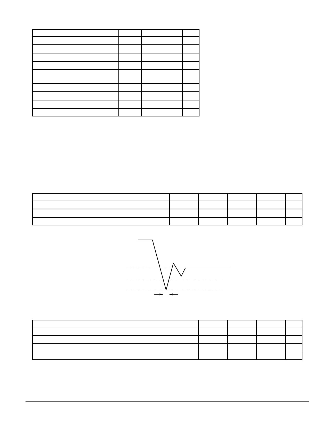
VIH
VSS
VSS – 1.0 V
20% tKHKH (MIN)
Figure 1. Undershoot Voltage
DC CHARACTERISTICS
Parameter
Input Leakage Current (0 V ≤ Vin ≤ VDD)
Output Leakage Current (0 V ≤ Vin ≤ VDD)
Output Low Voltage (IOL = + 8.0 mA)
Output High Voltage (IOH = – 4.0 mA)
Symbol
Min
Ilkg(I)
—
Ilkg(O)
—
VOL
—
VOH
2.4
Max
Unit
± 1.0
µA
± 1.0
µA
0.4
V
—
V
MCM72F8•MCM72F9
6
MOTOROLA FAST SRAM
Share Link: 