MCM72F10DG12 View Datasheet(PDF) - Motorola => Freescale
Part Name
Description
Manufacturer
MCM72F10DG12 Datasheet PDF : 11 Pages
| |||
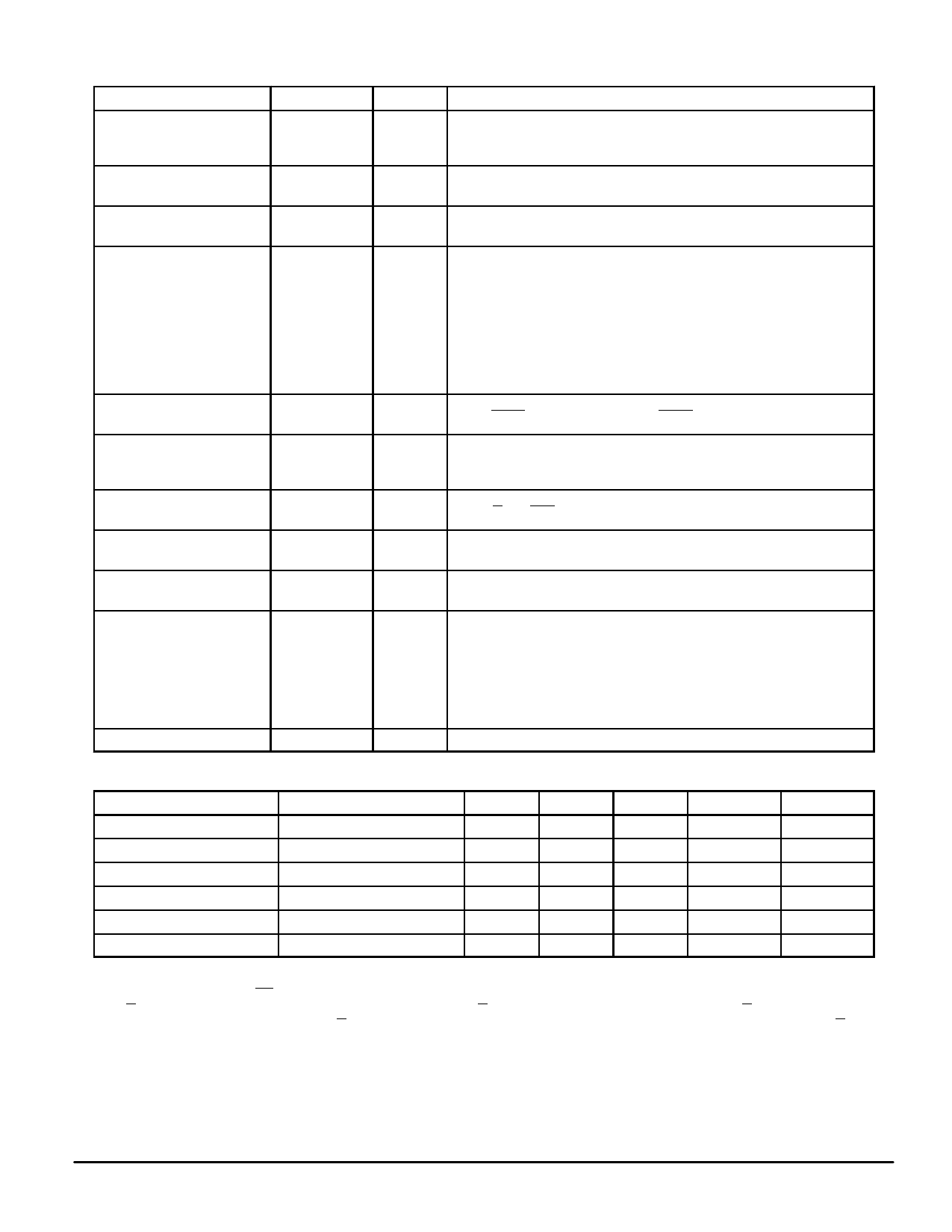
PIN DESCRIPTIONS
Pin Locations
59, 61, 62, 64, 65, 67, 68, 70,
71, 72, 143, 145, 146, 148,
149, 151, 152, 154, 155
156
Symbol
A0 – A18
ADSP
15, 31, 44, 86, 92, 105, 121,
134
2, 3, 5, 6, 8, 9, 11, 12, 14, 17,
18, 20, 21, 23, 24, 26, 27, 32,
34, 35, 37, 38, 40, 41, 43, 46,
47, 49, 50, 52, 53, 55, 56, 87,
89, 90, 93, 95, 96, 98, 99,
101, 102, 104, 107, 108, 110,
111, 115, 116, 118, 119, 122,
124, 125, 127, 128, 130, 131,
133, 136, 137, 139, 140
83, 167
DP0 – DP7
DQ0 – DQ63
E0, E1
82, 166
G0, G1
29, 74, 113, 158
76, 77, 79, 80, 160, 161, 163,
164
4, 16, 33, 45, 57, 69, 94, 106,
123, 135, 147, 165
1, 7, 10, 13, 19, 22, 25, 28,
30, 36, 39, 42, 48, 51, 54, 60,
63, 66, 73, 75, 78, 81, 84, 85,
88, 91, 97, 100, 103, 109,
112, 114, 117, 120, 126, 129,
132, 138, 141, 144, 150, 153,
157, 159, 162, 168
58, 142
K0 – K3
W0 – W7
VDD
VSS
NC
Type
Input
Description
Synchronous Address Inputs: These inputs are registered and must meet
setup and hold times.
Input
Synchronous Addresss Status Controller: Initiates read, write, or chip
deselect cycle.
Synchronous Parity Data Inputs/Outputs.
I/O
Synchronous Data Inputs/Outputs.
Input
Input
Input
Input
Supply
Synchronous Chip Enable: Active low to enable chip. Negated high —
blocks ADSP or deselects chip when ADSC is asserted.
Asynchronous Output Enable Input:
Low — enables output buffer.
High — DQx pins are high impedance.
Clock: This signal registers the address, data in, and all control signals
except G and LBO.
Synchronous Byte Write Inputs: x refers to the byte being written (byte a,
b).
Power Supply: 3.3 V + 10%, – 5%. Must be connected on all modules.
Supply Ground.
No Connection: There is no connection to the chip.
DATA RAM MCM69F618A SYNCHRONOUS TRUTH TABLE (See Notes 1, 2, 3, and 4)
Next Cycle
Address Used
E
ADSP
G
DQx
WRITE
Deselect
None
1
0
X
High–Z
X
Begin Read
External Address
0
0
0
DQ
Read
Read
Current
X
1
1
High–Z
Read
Read
Current
X
1
0
DQ
Read
Begin Write
External
0
0
X
High–Z
Write
Write
Current
X
1
X
High–Z
Write
NOTES:
1. X = don’t care, 1 = logic high, 0 = logic low.
2. Write is defined as any Wx low.
3. G is an asynchronous signal and is not sampled by the clock K. G drives the bus immediately (tGLQX) following G going low.
4. On write cycles that follow read cycles, G must be negated prior to the start of the write cycle to ensure proper write data setup times. G must
also remain negated at the completion of the write cycle to ensure proper write data hold times.
MCM72F10
4
MOTOROLA FAST SRAM
Share Link: 