MIC29310 View Datasheet(PDF) - Micrel
Part Name
Description
Manufacturer
MIC29310 Datasheet PDF : 12 Pages
| |||
MIC29310/29312
Micrel
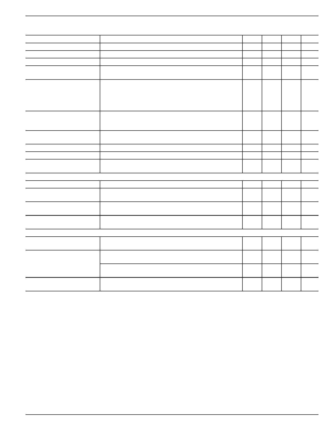
Electrical Characteristics(Note 11)
TJ = 25°C, bold values indicate 0°C ≤ TJ ≤ +125°C; unless noted
Parameter
Condition
Output Voltage
Line Regulation
Load Regulation
ΔVO / ΔT
ppm/°C
10mA ≤ IO ≤ IFL, (VOUT + 1V) ≤ VIN ≤ 8V, Note 4
IO = 10mA, (VOUT + 1V) ≤ VIN ≤ 16V
VIN = VOUT + 1V, 10mA ≤ IOUT ≤ IFULL LOAD, Notes 4, 8
Output Voltage Temperature Coefficient, Note 8
Dropout Voltage
Ground Current
IGNDDO Ground Pin
Current at Dropout
ΔVOUT = –1%, Note 5
IO = 100mA
IO = 750mA
IO = 1.5A
IO = 3A
IO = 750mA, VIN = VOUT + 1V
IO = 1.5A
IO = 3A
VIN = 0.5V less than specified VOUT. IOUT = 10mA
Current Limit
Minimum Load Current
VOUT = 0V, Note 6
en, Output Noise Voltage
(10Hz to 100kHz) IL = 100mA
Reference (MIC29312 only)
CL = 10µF
CL = 33µF
Reference Voltage
Adjust Pin Bias Current
10mA ≤ IO ≤ IFL, VOUT + 1V ≤ VIN ≤ 8V, Note 4
Reference Voltage
ppm/°C Temperature Coefficient
Adjust Pin Bias Current
Temperature Coefficient
Enable Input (MIC29312 only)
Input Logic Voltage
Enable Pin Input Current
Note 9
low (off)
high (on)
VEN = VIN
VEN = 0.8V
Regulator Output
Current in Shutdown
Note 10
Min Typ Max Units
–2
2
%
0.06 0.5
%
0.2
1
%
20
100
80
200
mV
220
mV
330
mV
600 1000 mV
5
20
mA
15
mA
60
150
mA
2
3
mA
3.0
3.8
A
7
10
mA
400
µVRMS
260
µVRMS
1.215
1.265 VMAX
40
80
nA
120
nA
20
0.1
nA/°C
0.8
V
2.4
V
15
30
µA
75
µA
–
2
µA
4
µA
10
µA
20
µA
Note 1. Exceeding the absolute maximum rating may damage the device.
Note 2. The device is not guaranteed to function outside its operating rating.
Note 3. Devices are ESD sensitive. Handling precautions recommended.
Note 4:
Note 5:
Note 6:
Note 7:
Full Load current is defined as 3A for the MIC29310/29312. For testing, VOUT is programmed to 5V.
Dropout voltage is defined as the input-to-output differential when the output voltage drops to 99% of its nominal value with VOUT + 1V applied
to VIN.
For this test, VIN is the larger of 8V or VOUT + 3V.
Ground pin current is the regulator quiescent current. The total current drawn from the source is the sum of the load current plus the ground
pin current.
Note 8: Output voltage temperature coefficient is defined as the worst case voltage change divided by the total temperature range.
Note 9: VREF ≤ VOUT ≤ (VIN – 1V), 2.4V ≤ VIN ≤ 16V, 10mA < IL ≤ IFL, TJ ≤ TJ(max).
Note 10: VEN ≤ 0.8V and VIN ≤ 8V, VOUT = 0.
Note 11: Specification for packaged product only.
November 2006
3
MIC29310/29312
Share Link: 