MIP803 View Datasheet(PDF) - Panasonic Corporation
Part Name
Description
Manufacturer
MIP803 Datasheet PDF : 3 Pages
| |||
Intelligent Power Devices (IPDs)
MIP803, MIP804
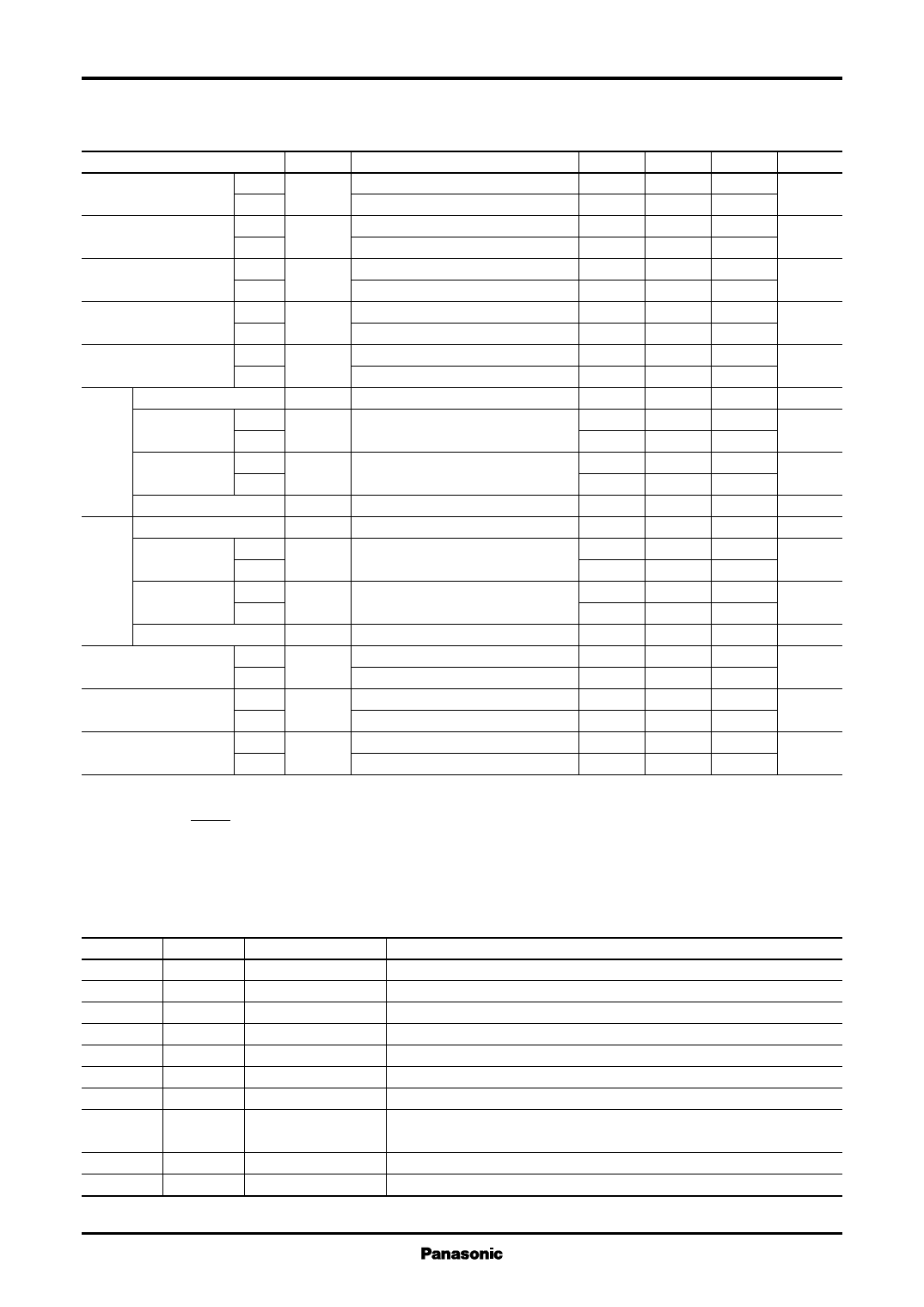
s Electrical Characteristics (VCC = 2.5V/1.2V, VENB = 2.5V/1.2V, GND = 0, TC = 25 ± 2°C)
Parameter
Symbol
Conditions
min
typ
max
Unit
Supply voltage
MIP803
MIP804 VCC
1.5
2.5
3.5
V
0.9
3.5
Output frequency
MIP803
MIP804 fOSC
Change of output
frequency
MIP803
MIP804 ∆fv Note)
High level input
voltage (ENB)
MIP803
MIP804 VIH
Low level input
voltage (ENB)
MIP803
MIP804 VIL
Breakdown voltage
VDSS
Saturation
Output current
MIP803
MIP804 IDS
RT = 390kΩ
RT = 240kΩ
RT = 390kΩ
RT = 240kΩ
VCC = 1.5 to 3.5V
VCC = 0.9 to 3.3V
VCC = 1.5 to 3.5V
VCC = 0.9 to 3.3V
IOFF(TR1) = 0.1mA
VDS(TR1) = 20V
119
140
161
kHz
195
230
265
−7
7
%
−15
15
1
V
0.8
0.3
V
0.1
200
V
70
mA
60
(TR1) ON-state
resistance
MIP803
MIP804 RON
IDS(TR1) = 10mA
6.5
10
Ω
15
Output
Off-leakage current
Breakdown voltage
Saturation
MIP803
current
MIP804
IOFF
VDSS
IDS
VDS(TR1) = 160V
IOFF(TR2) = 0.1mA
VDS(TR2) = 20V
2
µA
200
V
15
mA
10
(TR2) ON-state
resistance
MIP803
MIP804 RON
IDS(TR2) = 10mA
0.5
0.75
1
kΩ
0.7
1
1.4
Off-leakage current
IOFF
Clime power the inside MIP803
voltage
MIP804 VCP
Statically consumption MIP803
current
MIP804 IC
Consumption current
MIP803
MIP804 ICC
VDS(TR2) = 160V
VCC = VENB = 1.5V, CCP = 1000pF, RT = 390kΩ
2
VCC = VENB = 0.9V, CCP = 1000pF, RT = 240kΩ
2
VCC = 3.5V, VENB = 0
VCC = 3.3V, VENB = 0
VCC = VENB = 3.5V, RT = 390kΩ
VCC = VENB = 3.3V, RT = 240kΩ
2
µA
V
0.1
µA
0.1
1
1.5
mA
1
1.5
Note: ∆fv: Caluculation is made as follows:
∆fv
=
(fosc
/
f1
+
2
f2
−
1)
×
100
MIP803 f1: fosc at VCC = 1.5V, f2: fosc at VCC = 3.5V
MIP804 f1: fosc at VCC = 0.9V, f2: fosc at VCC = 3.5V
s Pin Descriptions
Pin No.
1
2
3
4
5
6
7
Symbol
GND
GND
CIL
GND
ELD
VCP
VCC
8
ENB
9
RT1
10
RT2
Pin Name
Description
GND pin
GND pin
GND pin
GND pin
Output for voltage step-up Drain pin of the voltage step-up MOS FET
GND pin
GND pin
Output for EL driving Drain pin of the EL drive MOS FET
Internal voltage step-up pin Capacitor connection pin for internal voltage step-up power supply
Power input pin
Power input pin
ENABLE pin
ENABLE signal input pin for controlling the EL driver (if ENB = H, the EL
driver becomes ON and if ENB = L/OPEN, it becomes OFF)
Internal oscillation output Internal oscillation circuit output pin
OSC resistor connecting pin OSC resistor connection pin for connecting the OSC resistor between RT1 and RT2
2
Share Link: 