MPC9774 View Datasheet(PDF) - Motorola => Freescale
Part Name
Description
Manufacturer
MPC9774 Datasheet PDF : 16 Pages
| |||
MPC9774
APPLICATIONS INFORMATION
MPC9774 Configurations
Configuring the MPC9774 amounts to properly configuring
the internal dividers to produce the desired output
frequencies. The output frequency can be represented by
this formula:
fOUT = fREF ⋅ M ÷ N
fREF
PLL
÷VCO_SEL
÷N
fOUT
÷M
where fREF is the reference frequency of the selected input
clock source (CCLKO or CCLK1), M is the PLL feedback
divider and N is a output divider. M is configured by the
FSEL_FB[0:1] and N is individually configured for each
output bank by the FSEL_A, FSEL_B and FSEL_C inputs.
The reference frequency fREF and the selection of the
feedback-divider M is limited by the specified VCO frequency
range. fREF and M must be configured to match the VCO
frequency range of 200 to 5001 MHz (VCC = 3.3V) in order to
achieve stable PLL operation:
fVCO,MIN (fREF ⋅ VCO_SEL ⋅ M) fVCO,MAX
The PLL post-divider VCO_SEL is either a divide-by-two
or a divide-by-four and can be used to situate the VCO into
the specified frequency range. This divider is controlled by
the VCO_SEL pin. VCO_SEL effectively extends the usable
input frequency range while it has no effect on the output to
reference frequency ratio. The output frequency for each
bank can be derived from the VCO frequency and the output
divider:
fQA[4:0] = fVCO ÷ (VCO_SEL ⋅ NA)
fQB[4:0] = fVCO ÷ (VCO_SEL ⋅ NB)
fQC[3:0] = fVCO ÷ (VCO_SEL ⋅ NC)
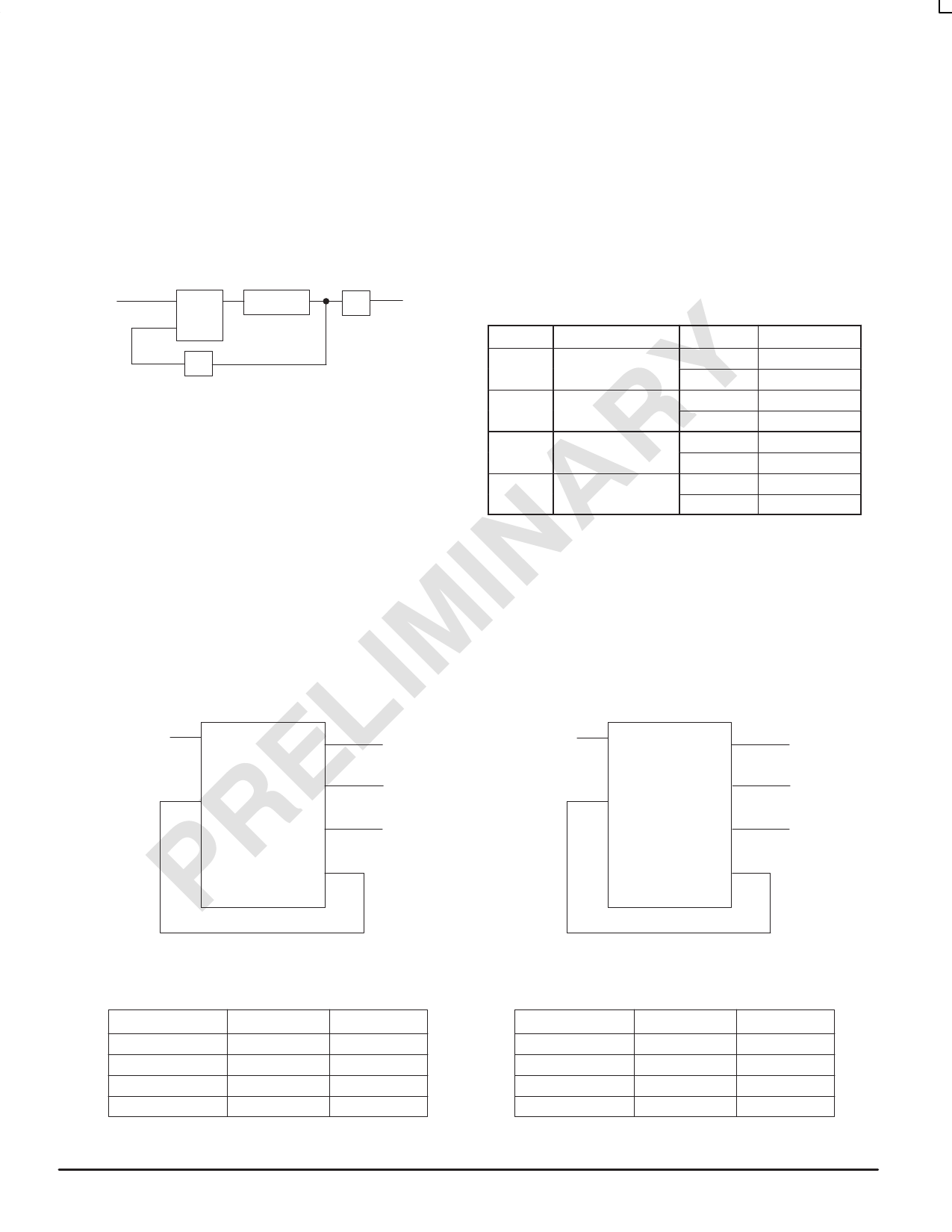
Table 11. MPC9774 Divider
Divider
Function
VCO_SEL
Values
M
PLL feedback
FSEL_FB[0:2]
NA
Bank A Output
Divider FSEL_A
NB
Bank B Output
Divider FSEL_B
NC
Bank C Output
Divider FSEL_C
÷2
8, 12, 16, 24
÷4
16, 24, 32, 48
÷2
4, 8
÷4
8, 16
÷2
4, 8
÷4
8, 16
÷2
8, 12
÷4
16, 24
1. The VCO frequency range for 2.5V operation is specified
from 200 to 400 MHz.
Table 11 shows the various PLL feedback and output
dividers. The output dividers for the three output banks allow
the user to configure the outputs into 1:1, 2:1, 3:2 and 3:2:1
frequency ratios. Figure 3 and Figure 4 display example
configurations for the MPC9774:
Figure 3. Example Configuration
fref = 20.83 MHz
CCLK0
CCLK1
0 CCLK_SEL
0 VCO_SEL
FB_IN
QA[4:0]
QB[4:0]
0 FSEL_A
QC[3:0]
1 FSEL_B
0 FSEL_C
10 FSEL_FB[1:0] QFB
MPC9774
20.83 MHz (Feedback)
125 MHz
62.5 MHz
62.5 MHz
MPC9774 example configuration (feedback of
QFB = 20.83 MHz, VCO_SEL = ÷2, M = 12, NA =
2, NB = 4, NC = 4, fVCO = 500 MHz).
Frequency range
Input
QA outputs
QB outputs
QC outputs
Min
8.33 MHz
50 MHz
25 MHz
25 MHz
Max
20.83 MHz
125 MHz
62.5 MHz
62.5 MHz
Figure 4. Example Configuration
fref = 25 MHz
CCLK0
CCLK1
0 CCLK_SEL
0 VCO_SEL
FB_IN
QA[4:0]
QB[4:0]
0 FSEL_A
QC[3:0]
1 FSEL_B
1 FSEL_C
01 FSEL_FB[1:0] QFB
MPC9774
25 MHz (Feedback)
100 MHz
50 MHz
33.3 MHz
MPC9774 example configuration (feedback of
QFB = 25 MHz, VCO_SEL = ÷2, M = 8, NA = 2,
NB = 4, NC = 6, fVCO = 400 MHz).
Frequency range
Input
QA outputs
QB outputs
QC outputs
Min
20 MHz
50 MHz
50 MHz
100 MHz
Max
48 MHz
120 MHz
120 MHz
200 MHz
MOTOROLA
8
TIMING SOLUTIONS
Share Link: 