MPC9855VF View Datasheet(PDF) - Motorola => Freescale
Part Name
Description
Manufacturer
MPC9855VF Datasheet PDF : 12 Pages
| |||
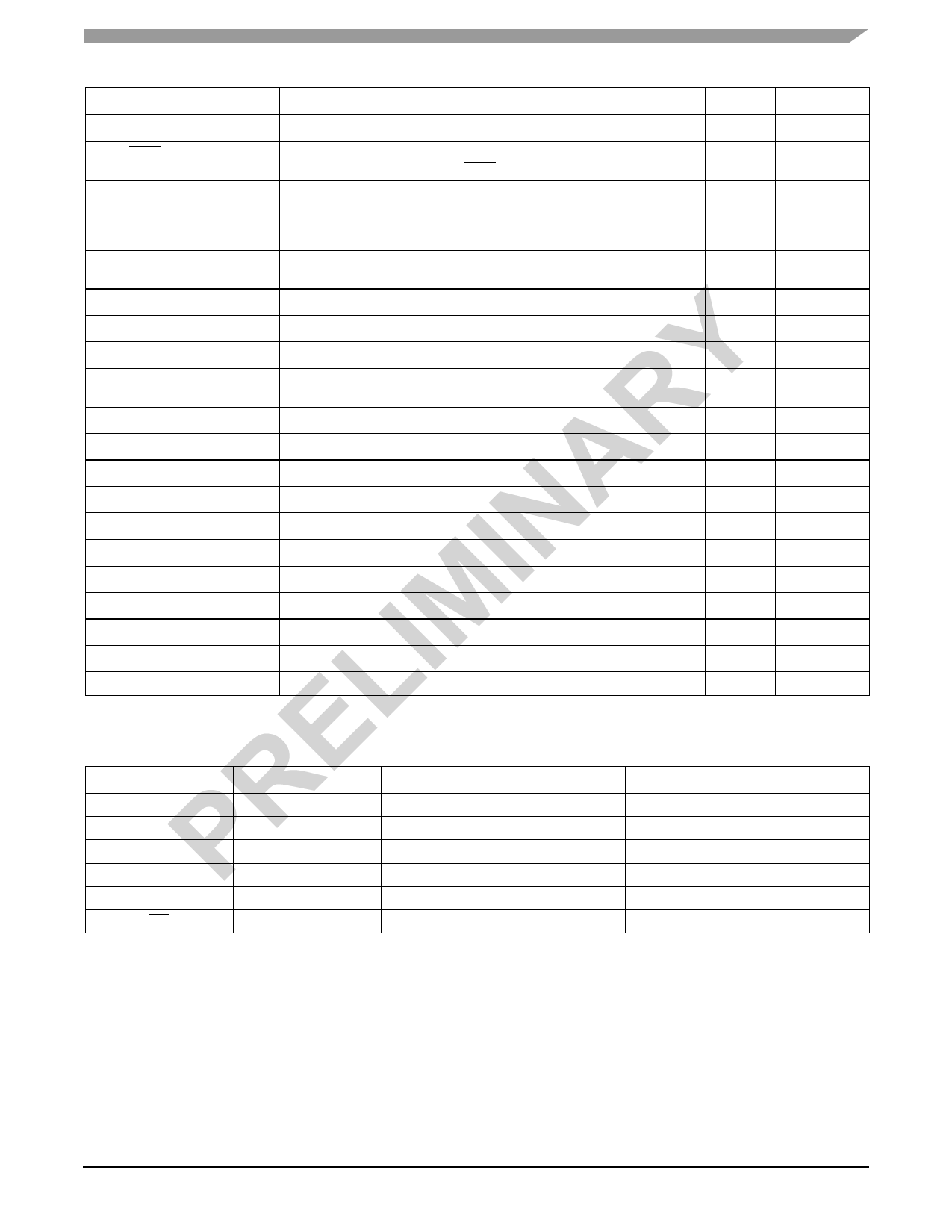
Table 1. Pin Configurations
Pin
CLK
I/O
Input
Type
Function
LVCMOS PLL reference clock input (pull-down)
PCLK, PCLK
QA0, QA1,
QA2, QA3
QB0, QB1,
QB2, QB3
REF_OUT0
REF_OUT1
XTAL_IN
Input
Output
LVPECL PLL reference clock input
(PCLK — pull-down, PCLK — pull-up and pull-down)
LVCMOS Clock Outputs
Output LVCMOS Reference Output (25 MHz or 33 MHz)
Input LVCMOS Crystal Oscillator Input Pin
XTAL_OUT
Output LVCMOS Crystal Oscillator Output Pin
CLK_SEL
Input LVCMOS Select between CLK and PCLK input (pull-down)
XTAL_SEL
REF_33 MHz
Input
Input
LVCMOS Select between External Input and Crystal Oscillator Input
(pull-down)
LVCMOS Selects 33MHz input (pull-down)
REF_OUT1_E
Input LVCMOS Enables REF_OUT! output (pull-down)
MR
Input LVCMOS Master Reset (pull-up)
PLL_BYPASS
Input LVCMOS Select PLL or static test mode (pull-up)
CLK_A[0:5](1)
Input LVCMOS Configures Bank A clock output frequency (pull-up)
CLK_B[0:5]1
Input LVCMOS Configures Bank B clock output frequency (pull-up)
VDD
—
— 3.3 V Supply
VDDA
—
— Analog Supply
VDDOA
—
— Output Supply — Bank A
VDDOB
—
— Output Supply — Bank B
GND
—
— Ground
1. Power PC bit ordering (bit 0 = msb, bit 5 = lsb).
Supply
VDD
VDD
Active/State
—
—
VDDOA
—
VDD
VDD
VDD
VDD
VDD
VDD
VDD
VDD
VDD
VDD
VDD
—
—
—
—
—
—
—
—
High
High
High
High
Low
High
—
—
—
—
—
—
—
Table 2. Function Table
Control
Default
0
CLK_SEL
0
CLK
XTAL_SEL
0
CLKx
PLL_BYPASS
0
Normal
REF_OUT1_E
0
Disables REF_OUT1
REF_33 MHz
0
Selects 25 MHz Reference
MR
1
Reset
CLK_A and CLK_B control output frequencies. Refer to Table 3 for specific device configuration
1
PCLK
XTAL
Bypass
Enables REF_OUT1
Selects 33 MHz Reference
Normal
Timing Solutions
Freescale Semiconductor
MPC9855
3
Share Link: 