MPC9855VF View Datasheet(PDF) - Motorola => Freescale
Part Name
Description
Manufacturer
MPC9855VF Datasheet PDF : 12 Pages
| |||
OPERATION INFORMATION
Output Frequency Configuration
The MPC9855 was designed to provide the commonly
used frequencies in PowerQUICC, PowerPC and other mi-
croprocessor systems. Table 3 lists the configuration values
that will generate those common frequencies. The MPC9855
can generate numerous other frequencies that may be useful
in specific applications. The output frequency (fout) may be
calculated by the following equation.
fout = 2000 / N
where fout is in MHz and N = 2 * CLK_x[0:5]
This calculation is valid for all values of N from 8 to 126.
Note that N = 15 is a modified case of the configuration inputs
CLK_x[0:5]. To achieve N = 15 CLK_x[0:5] is configured to
00111 or 7.
Crystal Input Operation
The MPC9855 features a fully integrated Pierce oscillator
to minimize system implementation costs. Other than the
addition of a crystal no external components are required
The crystal selection should be 25 MHz, parallel resonant
type with a load specification of CL = 10 pF.
The crystal should be located as close to the MPC92469
XTAL_IN and XTAL_OUT pins as possible to avoid any board
level parasitic.
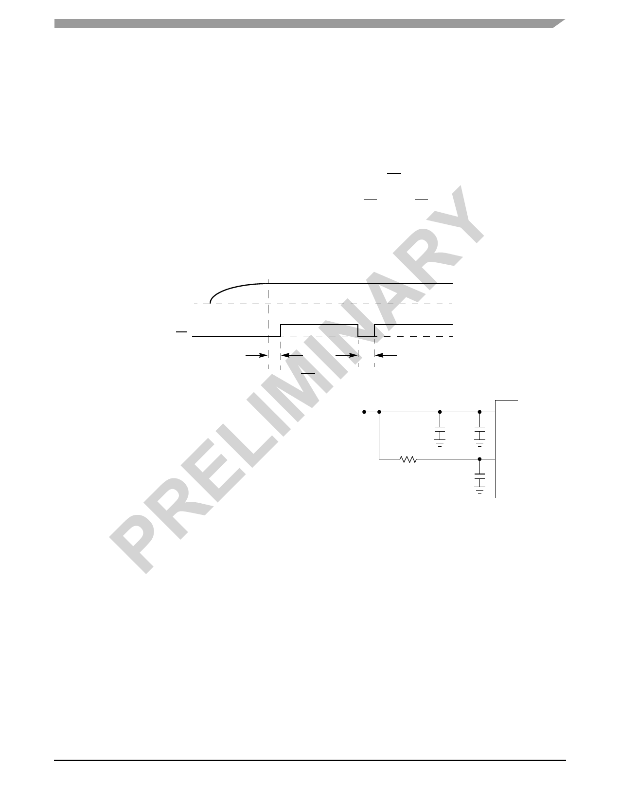
Power-Up and MR Operation
Figure 2 defines the release time and the minimum pulse
length for MR pin. The MR release time is based upon the
power supply being stable and within VDD specifications. See
Table 10 for actual parameter values. The MPC9855 may be
configured after release of reset and the outputs will be stable
for use after lock indication is obtained.
VDD
MR
treset_rel
treset_pulse
Figure 2. MR Operation
Power Supply Bypassing
The MPC9855 is a mixed analog/digital product. The
architecture of the XC9855 supports low noise signal
operation at high frequencies. In order to maintain its superior
signal quality, all VDD pins should be bypassed by
high-frequency ceramic capacitors connected to GND. If the
spectral frequencies of the internally generated switching
noise on the supply pins cross the series resonant point of an
individual bypass capacitor, its overall impedance begins to
look inductive and thus increases with increasing frequency.
The parallel capacitor combination shown ensures that a low
impedance path to ground exists for frequencies well above
the noise bandwidth.
VDD
VDD
22 µF 0.1 µF
MPC9855
15 Ω
VDDA
0.1 µF
Figure 3. VCC Power Supply Bypass
Power Consumption
The total power consumption of the MPC9855 may be
calculated by the following formula:
P = VDD * (IDD + IDDA + IDDOC) +
(CPD * frequency * * 4 * VDDOA**2) +
(CPD * frequency * 4 * VDDOB**2)
where frequency is the programmed output frequency for
bank A and bank B.
Timing Solutions
Freescale Semiconductor
MPC9855
5
Share Link: 