MPC9855VF View Datasheet(PDF) - Motorola => Freescale
Part Name
Description
Manufacturer
MPC9855VF Datasheet PDF : 12 Pages
| |||
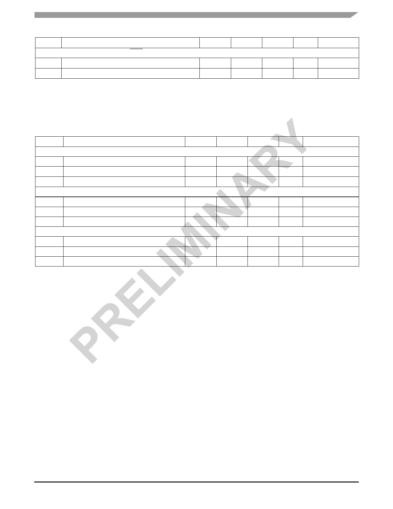
Table 7. LVPECL DC Characteristics (TA = –40°C to 85°C)(1)
Symbol
Characteristics
Min
Differential LVPECL clock inputs (CLK1, CLK1) for VDD = 3.3 V ± 0.5%
VPP Differential Voltage(2) (peak-to-peak)
(LVPECL)
250
VCMR Differential Input Crosspoint Voltage(3)
(LVPECL)
1.0
Typ
Max
Unit
Condition
mV
VDD – 0.6
V
1. AC characteristics are design targets and pending characterization.
2. VPP is the minimum differential input voltage swing required to maintain AC characteristics including tPD and device-to-device skew.
3. VCMR (AC) is the crosspoint of the differential input signal. Normal AC operation is obtained when the crosspoint is within the VCMR (AC)
range and the input swing lies within the VPP (AC) specification. Violation of VCMR (AC) or VPP (AC) impacts the device propagation delay,
device and part-to-part skew.
Table 8. LVCMOS I/O DC Characteristics (TA = –40°C to 85°C)
Symbol
Characteristics
Min
LVCMOS for VDD = 3.3 V ± 5%
VIH Input High Voltage
2.0
VIL
Input Low Voltage
IIN
Input Current(1)
LVCMOS for VDD = 3.3 V ± 5%, VDDOA = 3.3 V ± 5%, VDDOB = 3.3 V ± 5%
VOH Output High Voltage
2.4
VOL Output Low Voltage
ZOUT Output Impedance
LVCMOS for VDD = 3.3 V ± 5%, VDDOA = 2.5 V ± 5%, VDDOB = 2.5 V ± 5%
VOH Output High Voltage
1.9
VOL Output Low Voltage
ZOUT Output Impedance
1. Inputs have pull-down resistors affecting the input current.
Typ
Max
Unit
Condition
VDD + 0.3
0.8
200
V LVCMOS
V LVCMOS
µA VIN = VDDL or GND
0.4
14 – 17
V
IOH = –12 mA
V
IOL = 12 mA
Ω
0.4
18 – 22
V
IOH = –10 mA
V
IOL = 10 mA
Ω
Timing Solutions
Freescale Semiconductor
MPC9855
7
Share Link: 