MSM64P164 View Datasheet(PDF) - Oki Electric Industry
Part Name
Description
Manufacturer
MSM64P164
Oki Electric Industry

MSM64P164 Datasheet PDF : 37 Pages
| |||
¡ Semiconductor
MSM64P164
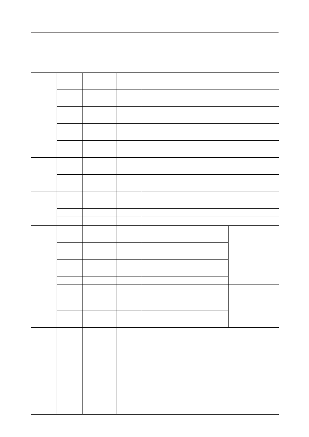
PIN DESCRIPTIONS
Basic Functions
Function Pin
32
42
Symbol
VSS
VDD1
Power
44
Supply
45
43
31
46,47
69
68
Oscillation
66
65
Ports
73 to 76
77 to 80
18 to 29
30
VDD2
VDD3
VDD
VPP
C1, C2
XT
XT
OSC1
OSC2
P1.0 to P1.3
P0.0 to P0.3
P2.0 to P4.3
BD
33
RT0
34
35
A/D
36
Converter 37
41
40
39
38
CRT0
RS0
CS0
IN0
RT1
RS1
CS1
IN1
Reset
70
RESET
Test
LCD
Drivers
71
72
1 to 17,
48 to 56
57 to 64
TST1
TST2
L0 to L25
L26/P5.0 to
L33/P6.3
Type
—
—
—
—
—
—
—
I
O
I
O
O
I
I/O
O
O
O
O
O
I
O
O
O
I
I
I
I
O
O
Description
0 V power supply
Bias output for driving LCD (+1.5 V), or positive power supply
at 1.5 V spec.
Bias output for driving LCD (+3.0 V), or positive power supply
at 3.0 V spec.
Bias output for driving LCD (+4.5 V).
Positive power supply for I/O port interface
Positive power supply for writing to PROM (+12.5 V)
Pins for connecting a capacitor for generating LCD driving bias.
32.768 kHz crystal connection pins
External 400 kHz oscillation resistor (ROS) connection pins
Output port (P1.0 : high current output)
Input port
Input-output ports
Output pin for the buzzer driver
Resistance temperature sensor
connection pin
Resistance/capacitance temperature
sensor connection pin
Reference resistor connection pin
Reference capacitor connection pin
RC oscillation pins
for A/D converter
(channel 0)
(CROSC0)
Input pin for RC oscillator circuit
Resistance temperature sensor
connection pin
Reference resistor connection pin
Reference capacitor connection pin
Input pin for RC oscillator circuit
RC oscillation pins
for A/D converter
(channel 1)
(CROSC1)
System reset input pin.
Setting this pin to "L" level puts this device into a reset state.
Them, setting this pin to "H" level starts executing an instruction
from address 000H.
This pin is internally pulled up to VDD.
Input pins for testing.
LCD driver pins
LCD driver pins, or output ports by mask option
5/37
Share Link: