MSM7654 View Datasheet(PDF) - Oki Electric Industry
Part Name
Description
Manufacturer
MSM7654 Datasheet PDF : 53 Pages
| |||
¡ Semiconductor
MSM7654
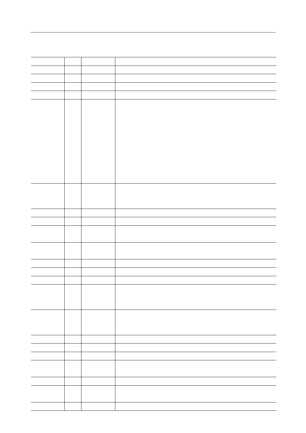
PIN DESCRIPTIONS
Pin
1
2
3
4
5 to 8
9
10
11
12
13
14
15
16
17 to 24
25 to 32
33
34
35 to 42
43
44
45
46
I/O Symbol
Description
DVDD
3.3 V digital power supply.
I/O
SDA
I2C interface data bus.
I
SCL
I2C interface clock bus.
I RGBMODE Input signal select pin. "0" : YCbCr / "1" : RGB, Internal pull-down.
I MODE[3:0] Operation mode select pin. However, sleep mode is valid while RGBMODE
is "0". Internal pull-down.
0000 : NTSC ITU-R BT.656
0001 : NTSC 27 MHz YCbCr
0010 : NTSC 24.52 MHz Square Pixel
0011 : NTSC 28.64 MHz 4Fsc
0101 : NTSC 13.5 MHz YCbCr
0110 : NTSC 12.27 MHz
0111 : NTSC 14.32 MHz
1000 : PAL ITU-R BT.656
1001 : PAL 27 MHz YcbCr
1010 : PAL 29.5 MHz Square Pixel
1101 : PAL 13.5 MHz
1110 : PAL 14.75 MHz
1111 : Sleep Mode (Valid only
when RGBMODE is "0")
I
MS
Master/slave operation selection in other modes than ITU-R BT.656. Internal
pull-down. "1" : Master / "0" : Slave
Only slave mode is selected in ITU-R BT.656 mode (input of "1" is invalid)
I/O GENLOCK GENLOCK signal I/O pin.
O CSYNC_L Composite sync output pin.
I/O VSYNC_L Vertical sync input/output pin (output mode in master mode/input mode in
slave mode)
I/O HSYNC_L Horizontal signal input/output pin (output mode in master mode/input mode
in slave mode)
I
BLANK_L Composite blank signal input pin.
DVDD 3.3 V digital power supply.
I
DGND Digital GND.
I CD0 to CD7 8-bit digital image chrominance signal data input pins at pixel rate
operation. Level conforms to ITU-R BT.601. R signal input pins in RGB input
mode. CD7 is MSB. Fixed to "0" when not used.
I YD0 to YD7 8-bit digital image data input pins at double pixel rate operation. 8-bit digital
luminance signal data input pins at pixel rate operation. Level conforms to
ITU-R BT.601. G signal input pins in RGB input mode. YD7 is MSB.
DGND Digital GND
DVDD 3.3 V digital power supply
I BD0 to BD7 B signal input pins in RGB input mode. Fixed to "0" when not used.
O
FOUT
Field information output pin (Odd Field : "1", Even Field : "0") (Polarity can
be changed by the internal register.)
I
RESET_L System reset pin.
I
TENB
Input pin for testing. Normally fixed to "0". Internal pull-down. The user
cannot use this pin.
I
CLKX2 Clock input pin.
5/52
Share Link: 