MSM9844 View Datasheet(PDF) - Oki Electric Industry
Part Name
Description
Manufacturer
MSM9844 Datasheet PDF : 32 Pages
| |||
¡ Semiconductor
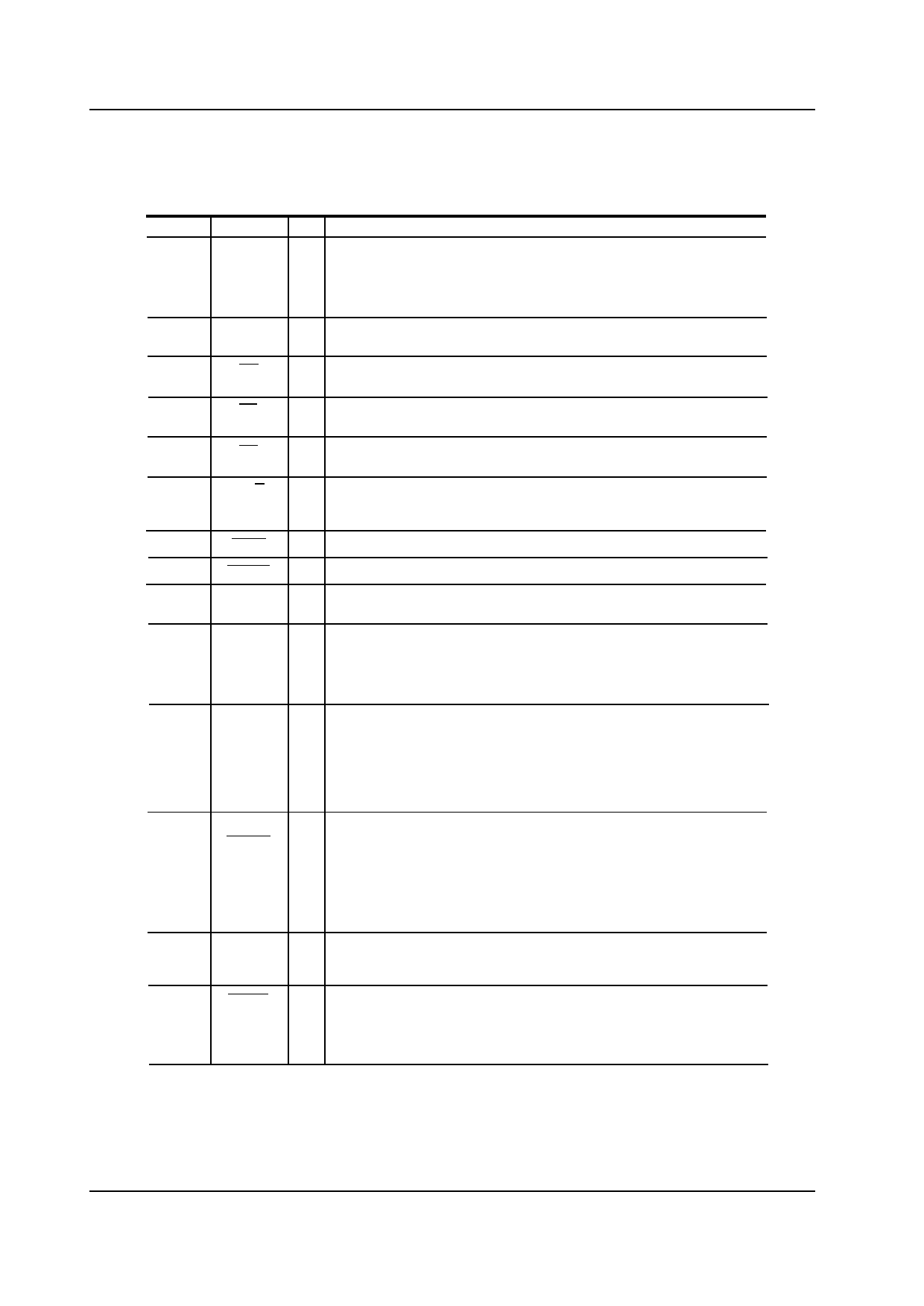
• Pin Description
MSM9844
Pin No.
11 - 14
16 - 19
1-4
6-9
38
39
40
41
42
32
35
36
37
34
51
50
Symbol
D15 to D8
I/O
Description
I/O
When 8-bit bus interface selected, you can define, by using a command,
these pins as input/output to/from external memory. When no definition
made, these pins are output mode.
When 16-bit bus interface selected, they are one half of bi-directional data
bus for data input / output from/to external micro-controller and memory.
D7 to D0
Another half of bi-directional data bus for data input/output from/to external
I / O micro-controller and memory and for status output.
WR
WRITE pulse input pin. Input "L" pulse before you can enter command
I and data to D15 to D0 pins.
RD
READ pulse input pin. Input "L" pulse before the LSI can output status and
I data to D15 to D0 pins.
CS
I
With this pin at "L" level, the LSI accepts WRITE or READ pulse input. At
"H" level the LSI would not accept WRITE or READ pulse.
D/C
While this pin being held "H", D15 to D0 pins are enabled to input/output
I sound data. While this pin being held "L", D7 to D0 pins are enabled to
input a command or output status data.
BUSY
O Output "L" level during playback/PAUSE operation.
CBUSY
O Output "L" level when the LSI is ready to accept a command.
EMP
O
"H" level output from this pin indicates FIFO memory is empty. You can
change this pin to "L" active by a command input.
MID
"H" level output from this pin indicates FIFO memory is more than half.
O During playback, voice synthesis starts when MID changes to "H" level.
You can change this pin to "L" active by a command input. This pin
outputs a synchro signal for voice data input / output when non-use of FIFO
is selected.
FUL /
DREQR
"H" level output from this pin indicates FIFO memory is full. During
playback operation this pin is held "H" and FIFO memory is write -disabled.
You can change this pin to "L" active by a command input.
O When DMA Transfer and stereo-playback selected by the command input,
the output from this pin becomes DMA Transfer request signal. The pin
outputs "H" when the right channel FIFO memory is empty. You can
change this pin to "L" active by a command input.
CH /
DACKR
When stereo-playback selected, write sound data to the right channel FIFO
at "H" level, while data to the left channel FIFO at "L" level. When monaural
playback selected, keep this pin "L". You can change this pin to "L" active by
I
a command input.
When DMA Transfer and stereo-playback selected by the command input,
this pin acknowledges the right channel DMA Transfer permission signal.
With this pin at "L" level the LSI enabled the /IOW pin to accept the signal.
You can change this pin to "H" active by a command input.
DREQL
Output "H" level to represent DMA Transfer request signal when FIFO gets
O empty. If stereo-playback selected, the pin outputs "H" level to represent
DMA Transfer request signal when the left channel FIFO gets empty.
DACKL
DMA Transfer Permission Acknowledgement signal. With this pin at "L"
level the LSI enables the /IOW pin to accept the signal. When stereo-
I playback selected, the pin acknowledges DMA Transfer permission signal
for the left channel FIFO. You can change this pin to "H" active by a
command input. When DMA Transfer is not in use, keep the pin "H".
Page4
Share Link: 