MSM9844 View Datasheet(PDF) - Oki Electric Industry
Part Name
Description
Manufacturer
MSM9844 Datasheet PDF : 32 Pages
| |||
¡ Semiconductor
MSM9844
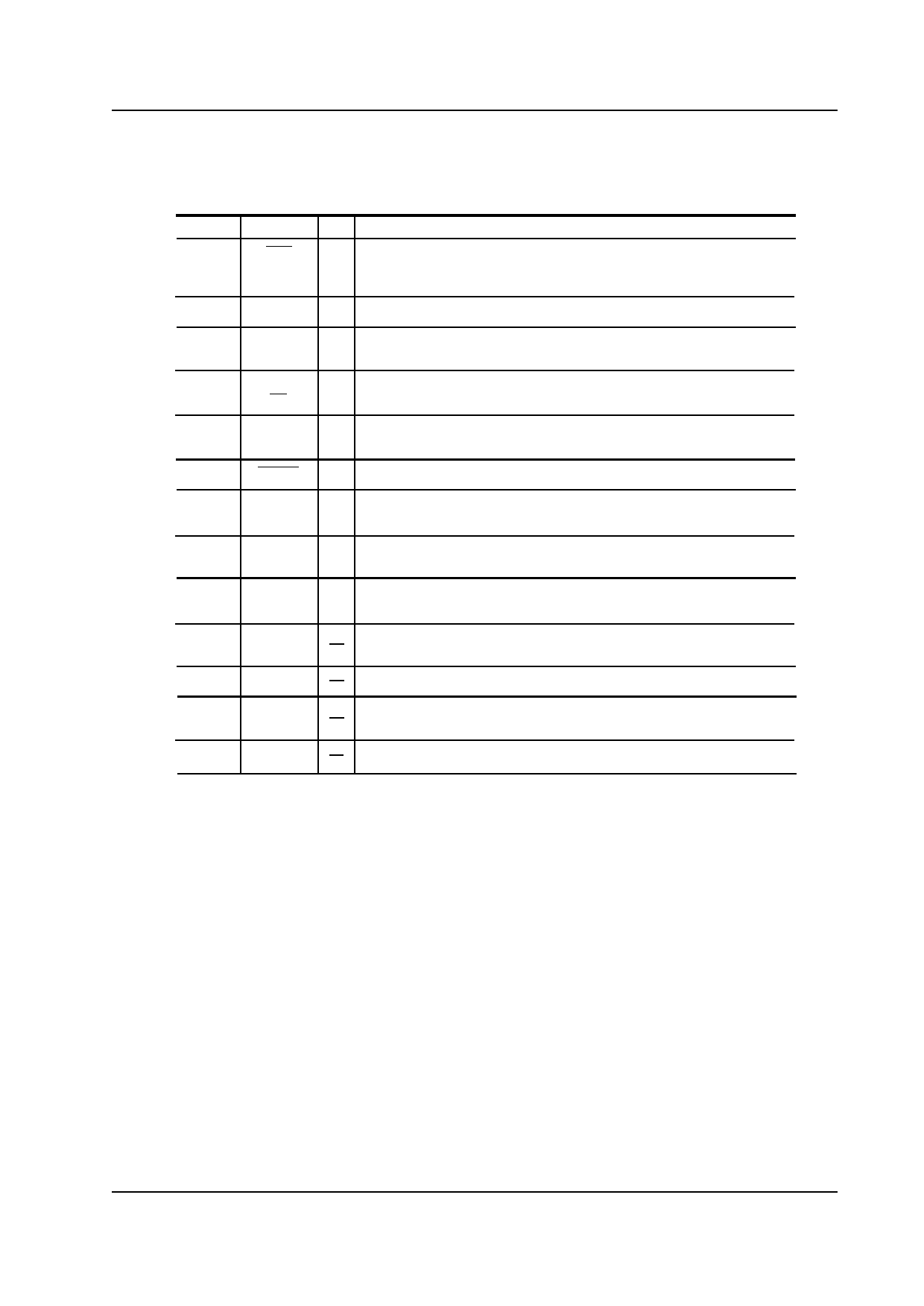
Pin No.
52
44
43
54
55
46
33
47,48
45,26
28
29
31
21,49
30
22
Symbol
IOW
I/O
Description
When DMA Transfer selected, the signal to start writing external memory
I data to the MSM9844 is entered to this pin.
When DMA Transfer is not use, keep the pin "H".
DASD
O 16-bit serial data output pin when the external DAC is in use.
SIOCK
Synchronizing clock signal for 16-bit serial data input/output when the
I / O external DAC is in use.
XT
I Pins wired to the oscillator, When the external clock is used, input the
XT
O clock signal to the XT pin and keep the /XT pin open.
VCK
I/O
Input/Output the sampling frequency in use. The signal is used as the
synchronizing signal when the external DAC is in use.
RESET
I "L" level input to this pin turns the LSI to the initial status.
TEST0,1
TEST2,3
I Pins for testing the LSI. Keep these pins "L".
AOUTL
O
The left channel output from the built-in LPF. Analog waveform output can
be directly connected to an amplifirer to drive a speaker.
AOUTR
O
The right channel output from the built-in LPF. Analog waveform output can
be directly connected to an amplifirer to drive a speaker.
DVDD
DGND
Digital power supply pin. Insert a 0.1µF or larger bypass capacitor
between this pin and the DGND pin.
Digital GND pin.
AVDD
Analog power supply pin. Insert a 0.1µF or larger bypass capacitor
between this pin and the AGND pin.
AGND
Analog GND pin.
Page5
Share Link: 