MT48LC1M16A1 View Datasheet(PDF) - Micron Technology
Part Name
Description
Manufacturer
MT48LC1M16A1 Datasheet PDF : 51 Pages
| |||
CAS Latency
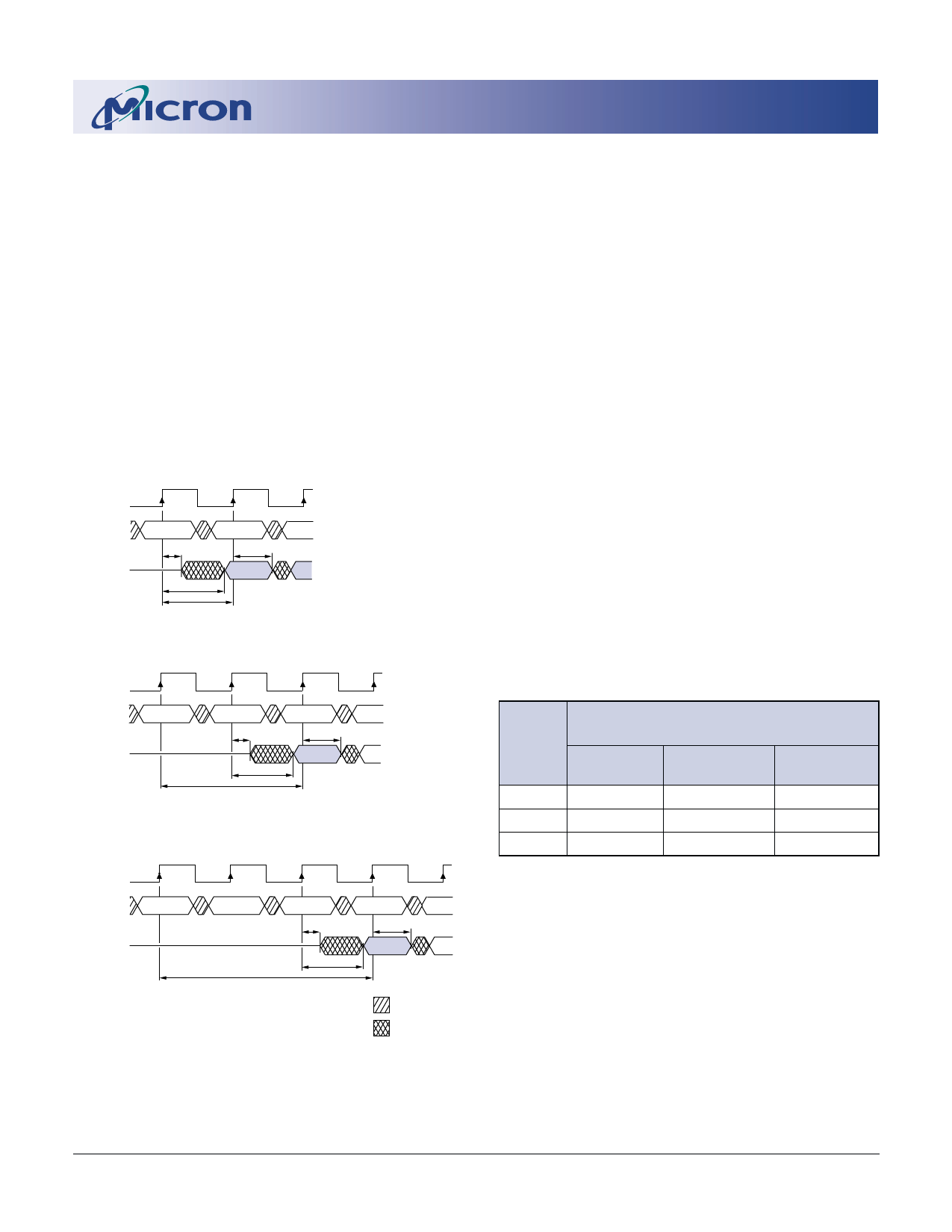
The CAS latency is the delay, in clock cycles, be-
tween the registration of a READ command and the
availability of the first piece of output data. The la-
tency can be set to 1, 2 or 3 clocks.
If a READ command is registered at clock edge n,
and the latency is m clocks, the data will be available by
clock edge n + m. The DQs will start driving as a result
of the clock edge one cycle earlier (n + m - 1), and
provided that the relevant access times are met, the
data will be valid by clock edge n + m. For example,
assuming that the clock cycle time is such that all
relevant access times are met, if a READ command is
registered at T0, and the latency is programmed to two
clocks, the DQs will start driving after T1 and the data
T0
T1
T2
CLK
COMMAND
DQ
READ
tLZ
tAC
NOP
tOH
DOUT
CAS Latency = 1
T0
T1
T2
T3
CLK
COMMAND
DQ
READ
NOP
tLZ
tAC
CAS Latency = 2
NOP
tOH
DOUT
CLK
COMMAND
T0
READ
DQ
T1
T2
NOP
NOP
tLZ
tAC
CAS Latency = 3
Figure 2
CAS Latency
T3
T4
NOP
tOH
DOUT
DON’T CARE
UNDEFINED
16Mb: x16
IT SDRAM
will be valid by T2, as shown in Figure 2. Table 2 below
indicates the operating frequencies at which each CAS
latency setting can be used.
Reserved states should not be used, as unknown
operation or incompatibility with future versions may
result.
Operating Mode
The normal operating mode is selected by setting
M7 and M8 to zero; the other combinations of values
for M7 and M8 are reserved for future use and/or test
modes. The programmed burst length applies to both
READ and WRITE bursts.
Test modes and reserved states should not be used
because unknown operation or incompatibility with
future versions may result.
Write Burst Mode
When M9 = 0, the burst length programmed via
M0-M2 applies to both READ and WRITE bursts; when
M9 = 1, the programmed burst length applies to READ
bursts, but write accesses are single-location (nonburst)
accesses.
Table 2
CAS Latency
SPEED
-6
-7
-8A
ALLOWABLE OPERATING
FREQUENCY (MHz)
CAS
CAS
CAS
LATENCY = 1 LATENCY = 2 LATENCY = 3
≤ 50
≤ 125
≤ 166
≤ 40
≤ 100
≤ 143
≤ 40
≤ 77
≤ 125
16Mb: x16 IT SDRAM
16MSDRAMx16IT.p65 – Rev. 5/99
8
Micron Technology, Inc., reserves the right to change products or specifications without notice.
©1999, Micron Technology, Inc.
Share Link: 