MCM69T618 View Datasheet(PDF) - Motorola => Freescale
Part Name
Description
Manufacturer
MCM69T618 Datasheet PDF : 10 Pages
| |||
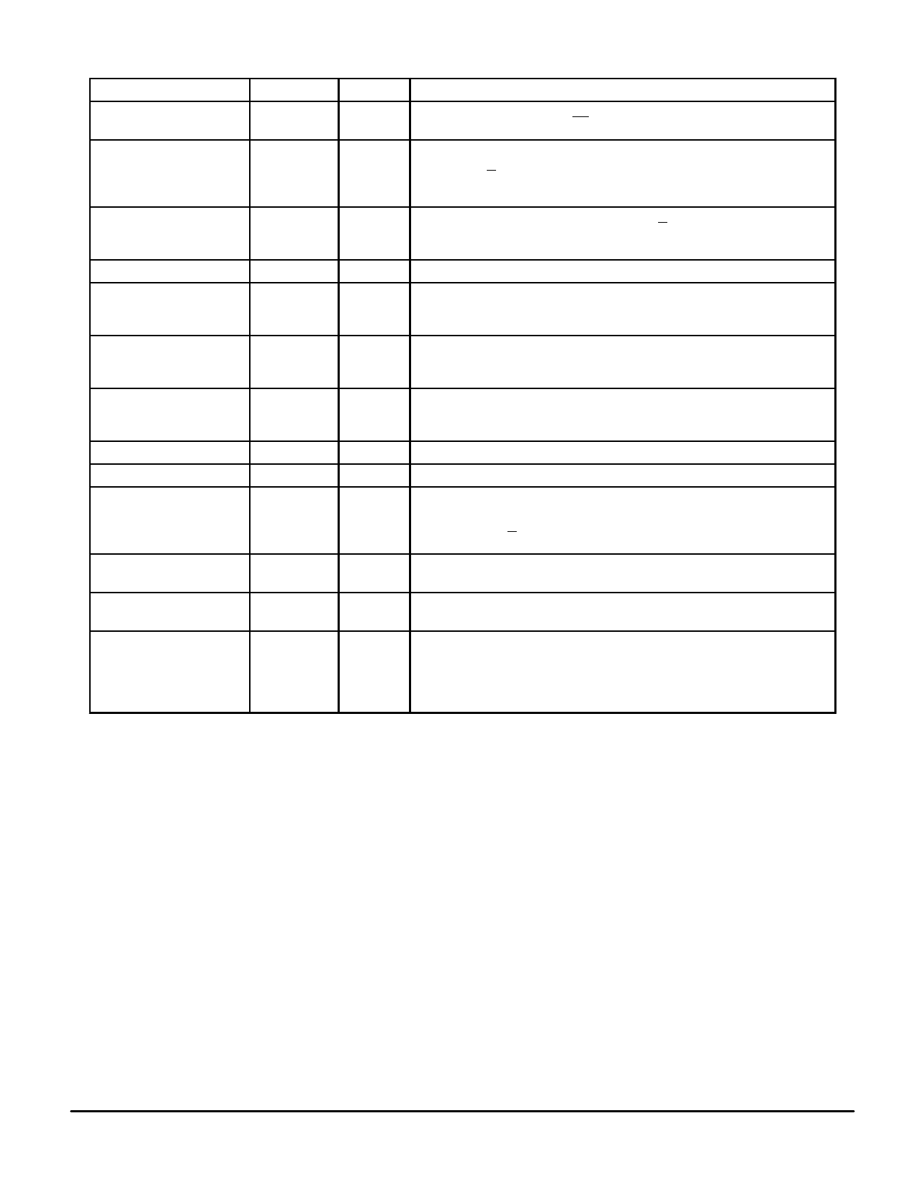
PIN DESCRIPTIONS
Pin Locations
42
Symbol
DE
8, 9, 12, 13, 18, 19, 22,
23, 24, 58, 59, 62, 63,
68, 69, 72, 73, 74
DQ1 – DQ18
86
G
89
K
39
MATCH
43
MG
32, 33, 34, 35, 36, 37,
SA
44, 45, 46, 47, 48, 80,
81, 82, 99, 100
97
SE0
98
SE1
87
SW
4, 11, 15, 20, 27, 41, 54,
61, 65, 70, 77, 91
5, 10, 17, 21, 26, 38, 40,
55, 60, 67, 71, 76, 90
1, 2, 3, 6, 7, 14, 16, 25,
28, 29, 30, 31, 49, 50, 51,
52, 53, 56, 57, 64, 66, 75,
78, 79, 83, 84, 85, 88, 92,
93, 94, 95, 96
VCC
VSS
NC
Type
Input
I/O
Input
Input
Output
Input
Input
Description
Data Enable Input: Latched on the rising clock edge, active low. The data input
register is only updated when DE is low.
Synchronous Data I/O: For write cycles, registered on the rising clock edge.
Two cycles after a read command, the read data is output on the DQ pins
provided that G is low. On the same cycle of a write command, the write data
is input on the DQ signals.
Output Enable: Asynchronous pin, active low. G must be low for read data to
be output two cycles after a read command. If G is high, the data output DQ
will remain in high impedance even if a read command occurs internally.
Clock: All the signals except G and MG are controlled by the clock.
Two cycles after a compare cycle and if MG is low, MATCH will be high if the
data presented to the DQ inputs matches the data stored in the RAM. MATCH
will be low if the data does not match.
Match Output Enable: Asynchronous pin, active low. When MG is low, the
MATCH output driver is on, otherwise the MATCH output driver is in high
impedance.
Synchronous Address Inputs: Registered on the rising clock edge. The
address pins select one of the 64K tag entries.
Input
Input
Input
Supply
Synchronous Chip Enable: Registered on the rising clock edge, active high.
Synchronous Chip Enable: Registered on the rising clock edge, active low.
Synchronous Write: Registered on the rising clock edge, active low. The SW
input specifies whether a read or write cycle is to occur when the chip is
enabled. A write command should not be issued within three cycles of a read
command unless G is high or output drive contention may occur.
Power Supply: 3.3 V + 10%, – 5%.
Supply Ground.
—
No Connection: There is no connection to the chip.
MCM69T618
4
MOTOROLA FAST SRAM
Share Link: 