HYB39S64800AT-10 View Datasheet(PDF) - Infineon Technologies
Part Name
Description
Manufacturer
HYB39S64800AT-10 Datasheet PDF : 53 Pages
| |||
HYB39S64400/800/160AT(L)
64MBit Synchronous DRAM
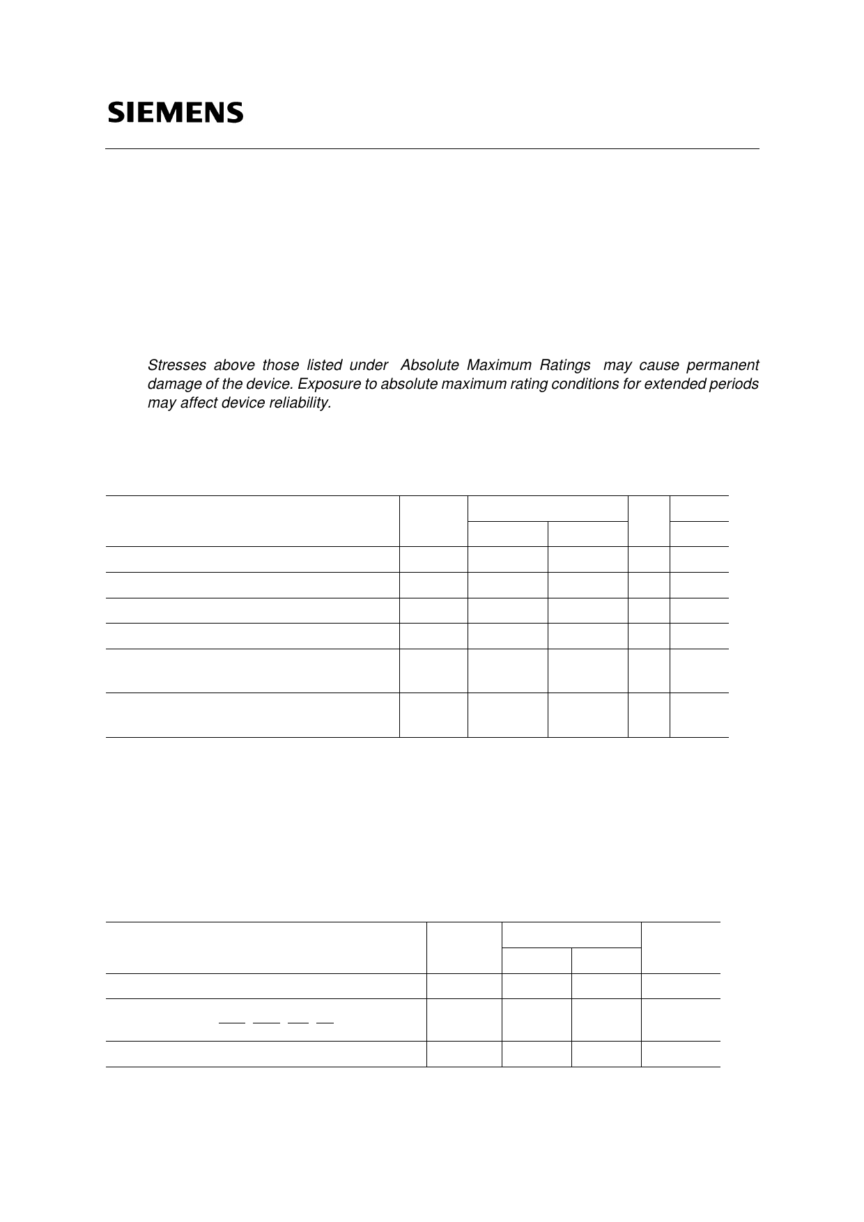
Absolute Maximum Ratings
Operating temperature range .........................................................................................0 to + 70 °C
Storage temperature range......................................................................................– 55 to + 150 °C
Input/output voltage .............................................................................................– 0.3 to Vdd+0.3 V
Power supply voltage VDD / VDDQ.......................................................................... – 0.3 to + 4.6 V
Power Dissipation............................................. ..........................................................................1 W
Data out current (short circuit) ................................................................................................ 50 mA
Note: Stresses above those listed under “Absolute Maximum Ratings” may cause permanent
damage of the device. Exposure to absolute maximum rating conditions for extended periods
may affect device reliability.
Recommended Operation and Characteristics for LV-TTL versions:
TA = 0 to 70 °C; VSS = 0 V; V V DD, DDQ = 3.3 V ± 0.3 V
Parameter
Input high voltage
Input low voltage
Output high voltage (IOUT = – 4.0 mA)
Output low voltage (IOUT = 4.0 mA)
Input leakage current, any input
(0 V < VIN < Vddq, all other inputs = 0 V)
Output leakage current
(DQ is disabled, 0 V < VOUT < Vdd)
Symbol
Limit Values
min.
max.
VIH
2.0
Vdd+0.3
VIL
– 0.3
0.8
VOH
2.4
–
VOL
–
0.4
II(L)
–5
5
Unit Notes
V 1, 2
V 1, 2
V
V
µA
IO(L)
–5
5
µA
Notes:
1. All voltages are referenced to VSS.
2. Vih may overshoot to Vdd + 2.0 V for pulse width of < 4ns with 3.3V. Vil may undershoot to
-2.0 V for pulse width < 4.0 ns with 3.3V. Pulse width measured at 50% points with amplitude measured peak
to DC reference.
Capacitance
TA = 0 to 70 °C; VDD = 3.3 V ± 0.3 V, f = 1 MHz
Parameter
Symbol
Input capacitance (CLK)
CI1
Input capacitance
CI2
(A0-A12, BA0,BA1,RAS, CAS, WE, CS, CKE, DQM)
Input / Output capacitance (DQ)
CIO
Values
min. max.
2.5
4.0
2.5
5.0
Unit
pF
pF
4.0
6.5
pF
Semiconductor Group
14
Share Link: 