MX23L8111 View Datasheet(PDF) - Macronix International
Part Name
Description
Manufacturer
MX23L8111 Datasheet PDF : 11 Pages
| |||
MX23L8111
PIN DESCRIPTION
Symbol
A0~A18
D0~D14
D15/A-1
CE
OE
Byte
VCC
VSS
NC
Pin Function
Address Inputs
Data Outputs
D15(Word Mode)/LSB Address (Byte
Mode)
Chip Enable Input
Output Enable Input
Word/Byte Mode Selection
Power Supply Pin
Ground Pin
No Connection
MODE SELECTION
CE OE Byte D15/A-1 D0~D7 D8~D15 Mode Power
HX X
X High Z High Z - Stand-by
LH X
X High Z High Z -
Active
L L H Output D0~D7 D8~D15 Word Active
L L L Input D0~D7 High Z Byte Active
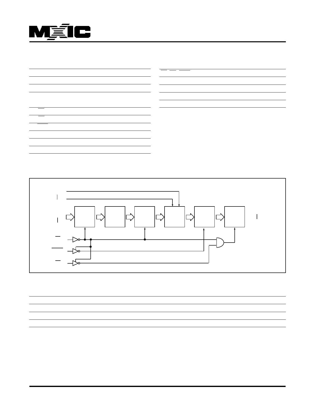
BLOCK DIAGRAM
A0/(A-1)
A2
A3
A18
CE
BYTE
OE
Address
Buffer
Memory
Array
Page
Buffer
Page
Decoder
Double
Word
Output
Buffer
D0
D15/(D7)
ABSOLUTE MAXIMUM RATINGS
Item
Voltage on any Pin Relative to VSS
Ambient Operating Temperature
Storage Temperature
Symbol
VIN
Topr
Tstg
Note: Minimum DC voltage on input or I/O pins is -0.5V.
During voltage transitions, inputs may undershoot VSS
to -1.3V for periods of up to 20ns. Maximum DC voltage
on input or I/O pins is VCC+0.5V. During voltage transi-
tions, input may overshoot VCC to VCC+2.0V for peri-
ods of up to 20ns.
P/N:PM0412
2
Ratings
-1.3V to VCC+2.0V (Note)
0° C to 70° C
-65° C to 125° C
REV. 2.3, JUN. 19, 2003
Share Link: 