NBXDDA016LN1TAG View Datasheet(PDF) - ON Semiconductor
Part Name
Description
Manufacturer
NBXDDA016LN1TAG Datasheet PDF : 6 Pages
| |||
NBXDDA016, NBXDDB016
Table 7. AC CHARACTERISTICS (VDD = 3.3 V ± 10%, GND = 0 V, TA = −40°C to +85°C) (Note 3)
Symbol
Characteristic
Conditions
Min.
Typ.
fCLKOUT
Output Clock Frequency
FSEL = HIGH
137.93
FSEL = LOW
133.33
Max.
Units
MHz
Df
Frequency Stability − NBXDDB016
Frequency Stability − NBXDDA016
(Note 4)
±20
ppm
±50
FNOISE
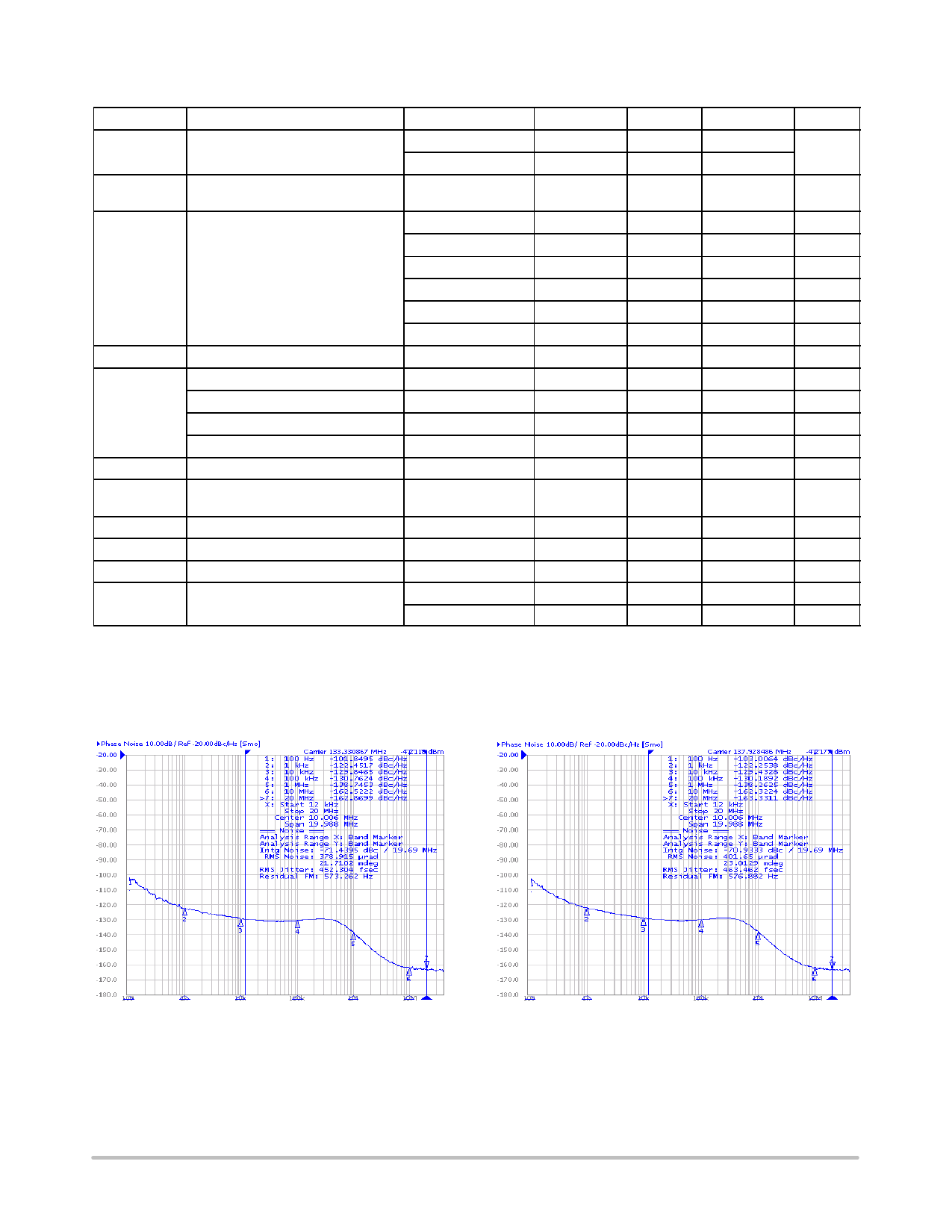
Phase−Noise Performance
fCLKout = 133.33 MHz/137.93 MHz
(See Figures 3 and 4)
100 Hz of Carrier
1 kHz of Carrier
10 kHz of Carrier
−102
−120
−126
dBc/Hz
dBc/Hz
dBc/Hz
100 kHz of Carrier
−126
dBc/Hz
1 MHz of Carrier
−134
dBc/Hz
10 MHz of Carrier
−162
dBc/Hz
tjit(F)
tjitter
RMS Phase Jitter
Cycle to Cycle, RMS
Cycle to Cycle, Peak−to−Peak
12 kHz to 20 MHz
1000 Cycles
1000 Cycles
0.4
0.9
ps
1.5
8
ps
10
30
ps
Period, RMS
10,000 Cycles
0.8
4
ps
Period, Peak−to−Peak
10,000 Cycles
7
20
ps
tOE/OD
tDUTY_CYCLE
Output Enable/Disable Time
Output Clock Duty Cycle
(Measured at Cross Point)
200
ns
48
50
52
%
tR
Output Rise Time (20% and 80%)
tF
Output Fall Time (80% and 20%)
tstart
Start−up Time
Aging
1st Year
Every Year After 1st
160
300
ps
160
300
ps
1
5
ms
3
ppm
1
ppm
NOTE: Device will meet the specifications after thermal equilibrium has been established when mounted in a test socket or printed circuit
board with maintained transverse airflow greater than 500 Ifpm. Electrical parameters are guaranteed only over the declared
operating temperature range. Functional operation of the device exceeding these conditions is not implied. Device specification limit
values are applied individually under normal operating conditions and not valid simultaneously.
3. Measurement taken with outputs terminated with 50 ohm to VDD. See Figure 5.
4. Parameter guarantees 10 years of aging. Includes initial stability at 25°C, shock, vibration, and first year aging.
Figure 3. Typical Phase Noise Plot @ 133.33 MHz
Figure 4. Typical Phase Noise Plot @ 137.93 MHz
http://onsemi.com
4
Share Link: 