NCP1378DR2 View Datasheet(PDF) - ON Semiconductor
Part Name
Description
Manufacturer
NCP1378DR2 Datasheet PDF : 16 Pages
| |||
NCP1378
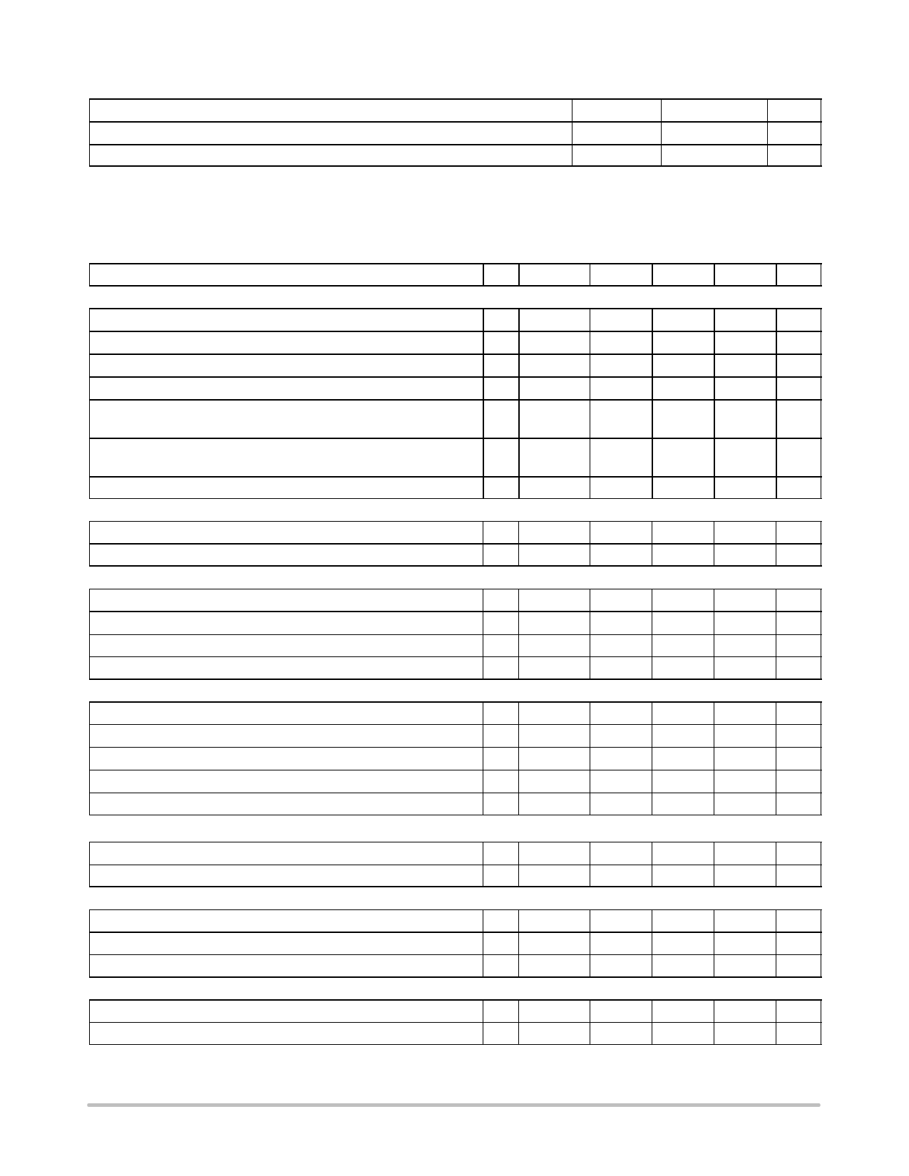
MAXIMUM RATINGS
Rating
Symbol
Value
Unit
ESD Capability, Machine Model
−
200
V
Maximum Voltage on Pin 8 (HV), Pin 6 (VCC) Decoupled to Ground with 10 mF
VHV
500
V
Stresses exceeding Maximum Ratings may damage the device. Maximum Ratings are stress ratings only. Functional operation above the
Recommended Operating Conditions is not implied. Extended exposure to stresses above the Recommended Operating Conditions may affect
device reliability.
ELECTRICAL CHARACTERISTICS (For typical values Tj = 25°C, for min/max values Tj = 0°C to +125°C, Max Tj = 150°C, VCC = 11 V
unless otherwise noted.)
Characteristic
Pin Symbol
Min
Typ
Max Unit
SUPPLY SECTION
VCC Increasing Level at which the Current Source Turns−Off
Minimum Operating Voltage after Turn−On
VCC Excursion between VCCON and VCCOFF
VCC Decreasing Level at which the Latchoff Phase Ends
Internal IC Consumption, No Output Load on Pin 5, FSW = 60 kHz
6
VCCON
7.8
6
VCCOFF
7.0
6
VCChyst
0.8
6
VCClatch
−
6
ICC1
−
8.4
9.0
V
7.5
8.2
V
−
−
−
5.5
−
V
1.0
1.3
mA
(Note 1)
Internal IC Consumption, 1.0 nF Output Load on Pin 5, FSW = 60 kHz
6
ICC2
−
1.6
2.0
mA
(Note 1)
Internal IC Consumption, Latchoff Phase, VCC = 6.0 V
INTERNAL STARTUP CURRENT SOURCE (Tj u 0°C)
High−Voltage Current Source, VCC = 7.8 V
High−Voltage Current Source, VCC = 0
DRIVE OUTPUT
6
ICC3
−
220
−
mA
8
IC1
8
IC2
2.4
4.0
6.0
mA
−
4.5
−
mA
Output Voltage Rise−Time @ CL = 1.0 nF, 10−90% of Output Signal
5
Tr
−
40
−
ns
Output Voltage Fall−Time @ CL = 1.0 nF, 10−90% of Output Signal
5
Tf
−
20
−
ns
Source Resistance
5
ROH
10
20
36
W
Sink Resistance
5
ROL
4.0
10
20
W
CURRENT COMPARATOR (Pin 5 not loaded)
Input Bias Current @ 1.0 V Input Level on Pin 3
Maximum Internal Current Setpoint
Propagation Delay from Current Detection to Gate OFF State
Leading Edge Blanking Duration
Internal Current Offset Injected on the CS Pin During OFF Time
3
IIB
3
ILimit
3
TDEL
3
TLEB
3
Iskip
−
0.02
−
mA
0.9
1.0
1.1
V
−
110
160
ns
−
340
−
ns
−
200
−
mA
OVERVOLTAGE SECTION (VCC = 11 V)
Sampling Delay After ON Time
OVP Internal Reference Level
FEEDBACK SECTION (VCC = 11 V, Pin 5 loaded by 1.0 kW)
Internal Pullup Resistor
Pin 3 to Current Setpoint Division Ratio
Internal Soft−Start
DEMAGNETIZATION DETECTION BLOCK
Input Threshold Voltage (Vpin 1 Decreasing)
Hysteresis (Vpin 1 Decreasing)
1
Tsample
−
4.5
−
ms
1
Vref
4.6
5.2
6.3
V
2
Rup
−
20
−
kW
−
Iratio
−
3.3
−
−
−
Tss
−
1.0
−
ms
1
Vth
1
VH
30
50
90
mV
−
20
−
mV
http://onsemi.com
4
Share Link: 