NCT47 View Datasheet(PDF) - ON Semiconductor
Part Name
Description
Manufacturer
NCT47 Datasheet PDF : 4 Pages
| |||
NCT47
ABSOLUTE MAXIMUM RATINGS*
Symbol
Parameter
Value
Unit
VDD
Supply Voltage
+7.0
V
VSS
Voltage on Any Pin with Respect to Supplies
(VSS – 0.3) to (VDD + 0.3)
V
TA
Operating Temperature Range
–40 to +125
°C
Tstg
Storage Temperature Range
–55 to +150
°C
Tsol
Lead Temperature (Soldering, 10 Seconds)
+260
°C
* Maximum Ratings are those values beyond which damage to the device may occur.
ELECTRICAL CHARACTERISTICS (TA = –40°C to +125°C, VDD = 2.7V to 4.4V, unless otherwise noted.)
Symbol
Characteristic
Min
Typ
VDD
Supply Voltage
2.7
—
IQ
Supply Current, Operating
—
35
AV
Average Slope of Output Voltage
—
10
TMPACY25 Temperature Accuracy at 25°C
TA = 25°C
–2.0
±0.5
TMPACY125 Temperature Accuracy
TA = 125°C
–3.0
—
TMPACY–40 Temperature Accuracy
TA = –40°C
—
1.5
VOUT–40
Output Voltage at –40°C
—
100
VOUT+25
Output Voltage at 25°C
730
750
VOUT+125
Output Voltage at 125°C
1720
1750
IOUT
Output Source and Sink Current
100
—
Max
4.4
60
—
+2.0
+3.0
—
—
770
1780
—
Unit
V
µA
mV/°C
°C
°C
°C
mV
mV
mV
µA
PIN DESCRIPTION
ÁÁÁÁÁÁÁÁPiÁÁÁÁn123NoÁÁÁÁ. ÁÁÁÁÁÁÁÁSVÁÁÁÁyVVOmDSUbSDÁÁÁÁTol ÁÁÁÁÁÁÁÁITGÁÁÁÁnerpmouuptÁÁÁÁneSdruaTptÁÁÁÁeuprrlmyeViSÁÁÁÁnoealnltasÁÁÁÁgoerOÁÁÁÁutpuÁÁÁÁtTerÁÁÁÁminÁÁÁÁal ÁÁÁÁDÁÁÁÁescrÁÁÁÁiptioÁÁÁÁn ÁÁÁÁÁÁÁÁÁÁÁÁÁÁÁÁÁÁÁÁÁÁÁÁÁÁÁÁÁÁÁÁÁÁÁÁÁÁÁÁ
DETAILED DESCRIPTION
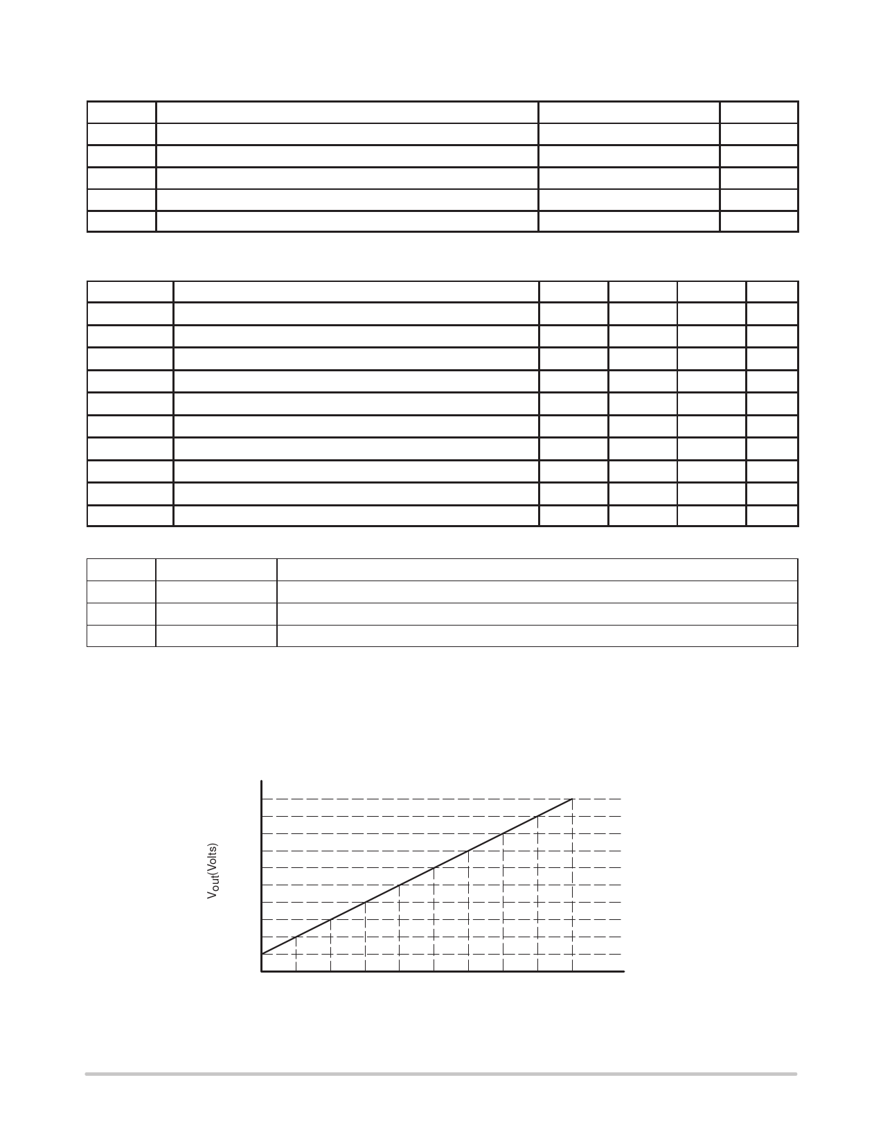
The NCT47 has an output voltage that varies linearly with
temperature in degrees Celsius. Figure 1 shows a plot of the
output voltage versus temperature for the NCT47. The
temperature slope is fixed at 10 mV/°C, and the output
voltage at 0°C is 500 mV.
VOUT = (10 mV/°C) (Temperature °C) + 500 mV
1.75
1.7
1.5
1.3
1.1
0.9
0.7
0.5
0.3
0.1
–40–30–20–10 0 10 20 30 40 50 60 70 80 90 100110120 125
Temperature (°C)
Figure 1. Output Voltage vs. Temperature
http://onsemi.com
2
Share Link: 