NCV8518A(2011) View Datasheet(PDF) - ON Semiconductor
Part Name
Description
Manufacturer
NCV8518A
(Rev.:2011)
(Rev.:2011)
ON Semiconductor

NCV8518A Datasheet PDF : 13 Pages
| |||
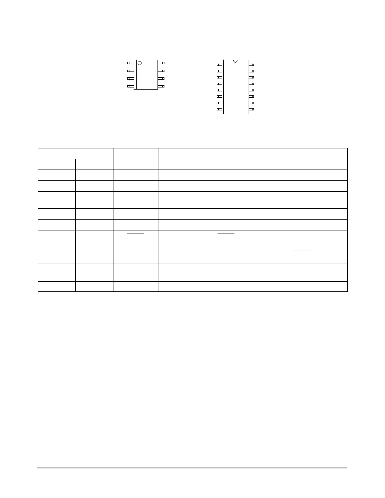
NCV8518A
PIN CONNECTIONS
SOIC−8 EP
1
Wake Up
8
RESET
GND
WDI
Delay
VOUT
ENABLE
VIN
SOIC−16 EP
1
NC
16
Wake Up
NC
RESET
GND
NC
NC
WDI
Delay
NC
NC
ENABLE
NC
NC
VOUT
VIN
PIN FUNCTION DESCRIPTION
Pin
SOIC−8 EP SOIC−16 EP
Symbol
4
8
VOUT
5
9
VIN
7
13
WDI
2
3
GND
6
11
ENABLE
8
3
−
1
EPAD
15
5
1, 2, 4, 6, 7,
10, 12, 14
16
EPAD
RESET
Delay
NC
Wake Up
EPAD
Description
Regulated output voltage.
Input supply voltage.
CMOS compatible Watchdog input. The watchdog function monitors the falling edge of
the incoming signal.
Ground connection.
ENABLE control for the IC. Positive logic. If ENABLE control will not be used, connect
this pin to VIN via a 20k current limiting resistor. Internal ESD protection structures will
clamp the maximum ENABLE voltage to approximately 21 V.
CMOS compatible output RESET goes low whenever VOUT drops by more than 7.0%
from nominal, or during the absence of a correct watchdog signal.
Buffered reference voltage used to create timing current for RESET and Watchdog
threshold frequency from RDelay.
No Connection.
Continuously generated signal that interrupts the microprocessor from sleep mode.
Connect to Ground potential or leave unconnected.
http://onsemi.com
2
Share Link: