NCV8518A View Datasheet(PDF) - ON Semiconductor
Part Name
Description
Manufacturer
NCV8518A Datasheet PDF : 13 Pages
| |||
NCV8518A
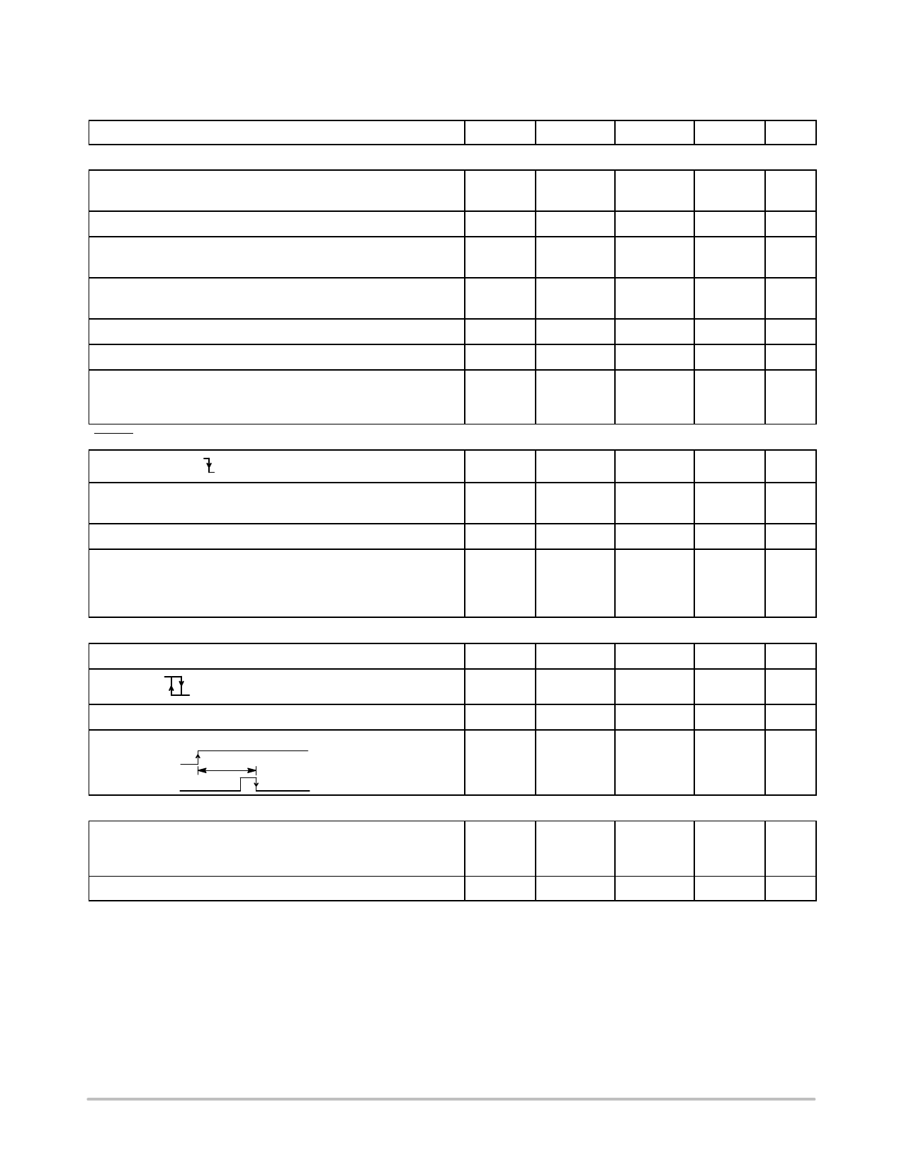
ELECTRICAL CHARACTERISTICS (-40°C ≤ TJ ≤ 150°C; 6.0 V ≤ VIN ≤ 28 V, 100 mA ≤ IOUT ≤ 150 mA, C2 = 1.0 mF, RDelay = 60 k;
unless otherwise specified.)
Characteristic
Symbol
Min
Typ
Max
Unit
Output
Output Voltage
VOUT
4.9
-2%
5.00
5.10
V
+2%
Dropout Voltage (VIN - VOUT, IOUT = 150 mA) (Note 5)
Load Regulation
(VIN = 13.5 V, 100 mA ≤ IOUT ≤ 150 mA)
Line Regulation
(6.0 V ≤ VIN ≤ 28 V, IOUT = 5.0 mA)
Current Limit
Thermal Shutdown (Guaranteed by Design)
Quiescent Current
(VIN = 13.5 V, IOUT = 100 mA, 150 mA, ENABLE = 2.0 V)
(ENABLE = 0 V, TA = +125°C)
RESET
Threshold Voltage
VDO
Regload
Regline
Ilim
TJmax
IQ
-
-
-
-
255
150
-
-
4.50
425
750
mV
5.0
30
mV
5.0
20
mV
400
-
mA
180
210
°C
mA
100
150
-
1.0
4.65
4.75
V
Output Low
(RLOAD = 10 k to VOUT, VOUT = 1.0 V)
Output High (RLOAD = 10 k to GND)
Power On Reset Delay Time
(VIN = 13.5 V, RDelay = 60 k, IOUT = 5.0 mA)
(VIN = 13.5 V, RDelay = 120 k, IOUT = 5.0 mA)
VIN = 13.5 V, RDelay = 500 k, IOUT = 5.0 mA)
Watchdog Input
Threshold
Hysteresis
-
-
0.2
0.4
V
-
VOUT - 0.4 VOUT - 0.2
-
V
tD
ms
2.0
3.0
4.0
-
6.0
-
-
25
-
WDIhigh
30
WDIhys
25
50
70
%VOUT
100
-
mV
Input Current (WDI = 6.0 V)
Wake Up Rising Edge to WDI Falling Edge Delay
Wake Up
WDI
-
-
0.1
2.0
mA
-
5.0
-
-
ms
ENABLE (Note 6)
Input Threshold
Logic Low
Logic High
Vth(EN)
-
2.0
V
-
0.8
-
-
Input Current (ENABLE = 2.0 V)
-
-
3.0
10
mA
5. Measured when the output voltage has dropped 2% from the nominal value.
6. If ENABLE is connected to VIN, a 20 kW resistor must be placed in series.
http://onsemi.com
5
Share Link: 