NE33284A-T1A View Datasheet(PDF) - NEC => Renesas Technology
Part Name
Description
Manufacturer
NE33284A-T1A Datasheet PDF : 10 Pages
| |||
NE33284A
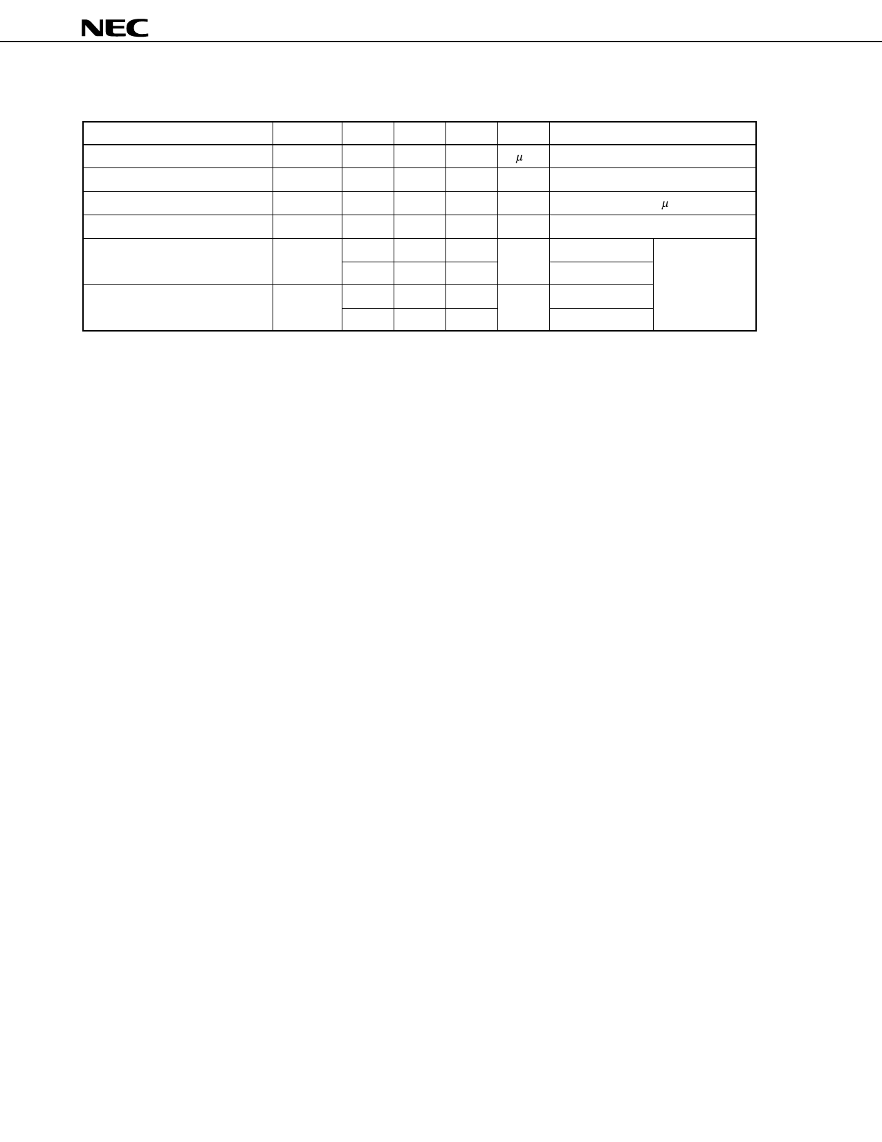
ELECTRICAL CHARACTERISTICS (TA = 25 ˚C)
PARAMETER
Gate to Source Leak Current
Saturated Drain Current
Gate to Source Cutoff Voltage
Transconductance
Noise Figure
Associated Gain
SYMBOL
IGSO
IDSS
VGS(off)
gm
NF
MIN.
15
–0.2
45
Ga
9.5
13.0
TYP.
0.5
40
–0.8
70
0.75
0.35
10.5
15.0
MAX.
10
80
–2.0
1.0
0.45
UNIT
µA
mA
V
mS
dB
dB
TEST CONDITIONS
VGS = –3 V
VDS = 2 V, VGS = 0
VDS = 2 V, ID = 100 µA
VDS = 2 V, ID = 10 mA
f = 12 GHz
f = 4 GHz
VDS = 2 V
ID = 10 mA
f = 12 GHz
f = 4 GHz
PRECAUTION: Avoid high static voltage and electric fields, because this device is Hetero Junction field effect
transistor with AlGaAs shottky barrier gate.
2
Share Link: 