SA572 View Datasheet(PDF) - Philips Electronics
Part Name
Description
Manufacturer
SA572 Datasheet PDF : 8 Pages
| |||
Philips Semiconductors RF Communications Products
Programmable analog compandor
Product specification
NE/SA572
ǒ Ǔ ǒ Ǔ VTIn
1
2
IG
)
1
2
IO
IS
*
VTIn
1
2
IG
*
1
2
IO
IS
V+
where
IIN
+
VIN
R1
R1 = 6.8kΩ
I1 = 140µA
I2 = 280µA
ǒ Ǔ ǒ Ǔ VTIn
I1 ) IIN
IS
*
VTIn
I2 *
I1 *
IS
IIN (2)
1
2
IG
)
1
2
IO
I1
140µA
where
IIN
+
VIN
R1
R1 = 6.8kΩ
I1 = 140µA
I2 = 280µA
IO is the differential output current of the gain
cell and IG is the gain control current of the
gain cell.
If all transistors Q1 through Q4 are of the
same size, equation (2) can be simplified to:
IO
+
2
I2
@
IIN @
IG *
1
I2
ǒ
I2
*
2I1Ǔ @ IG
The first term of Equation 3 shows the
multiplier relationship of a linearized two
quadrant transconductance amplifier. The
second term is the gain control feedthrough
due to the mismatch of devices. In the
design, this has been minimized by large
matched devices and careful layout. Offset
voltage is caused by the device mismatch
and it leads to even harmonic distortion. The
offset voltage can be trimmed out by feeding
a current source within ±25µA into the THD
trim pin.
The residual distortion is third harmonic
distortion and is caused by gain control
ripple. In a compandor system, available
control of fast attack and slow recovery
improve ripple distortion significantly. At the
unity gain level of 100mV, the gain cell gives
THD (total harmonic distortion) of 0.17% typ.
Output noise with no input signals is only 6µV
in the audio spectrum (10Hz-20kHz). The
output current IO must feed the virtual ground
input of an operational amplifier with a
resistor from output to inverting input. The
non-inverting input of the operational
amplifier has to be biased at VREF if the
output current IO is DC coupled.
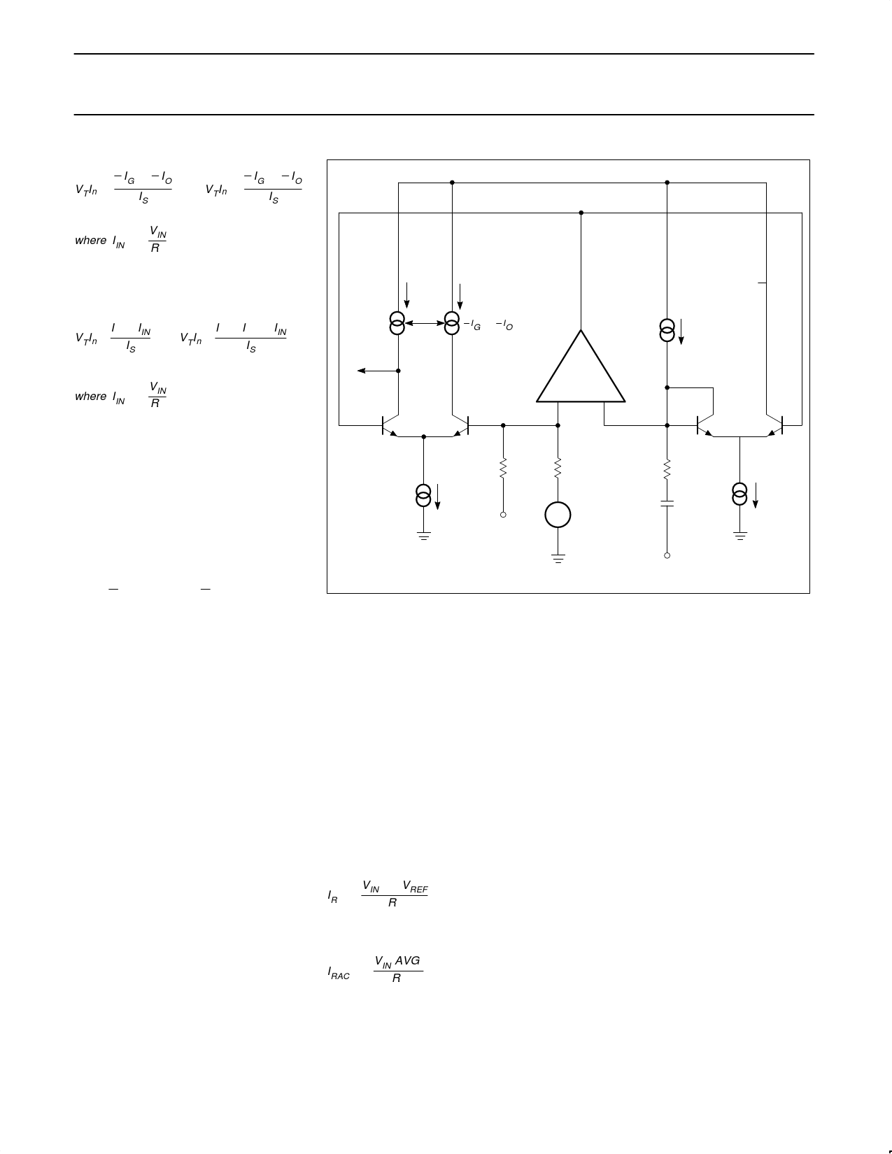
IO
Q4
Q3
A1
+
–
Q1
Q2
R1
6.8k
IG
I2
280µA
THD
TRIM
VREF
VIN
(3)
Figure 1. Basic Gain Cell Schematic
Rectifier
The rectifier is a full-wave design as shown in
Figure 2. The input voltage is converted to
current through the input resistor R2 and
turns on either Q5 or Q6 depending on the
signal polarity. Deadband of the voltage to
current converter is reduced by the loop gain
of the gain block A2. If AC coupling is used,
the rectifier error comes only from input bias
current of gain block A2. The input bias
current is typically about 70nA. Frequency
response of the gain block A2 also causes
second-order error at high frequency. The
collector current of Q6 is mirrored and
summed at the collector of Q5 to form the full
wave rectified output current IR. The rectifier
transfer function is
IR
+
VIN
* VREF
R2
(4)
If VIN is AC-coupled, then the equation will be
reduced to:
IRAC
+
VIN(AVG)
R2
The internal bias scheme limits the maximum
output current IR to be around 300µA. Within a
±1dB error band the input range of the rectifier
is about 52dB.
October 7, 1987
5
Share Link: 