SA572F View Datasheet(PDF) - Philips Electronics
Part Name
Description
Manufacturer
SA572F Datasheet PDF : 8 Pages
| |||
Philips Semiconductors RF Communications Products
Programmable analog compandor
Product specification
NE/SA572
VOUT
VIN
+
2
I1
@
R3 @ VIN(AVG)
R2 @ R1
(5)
(I1=140µA)
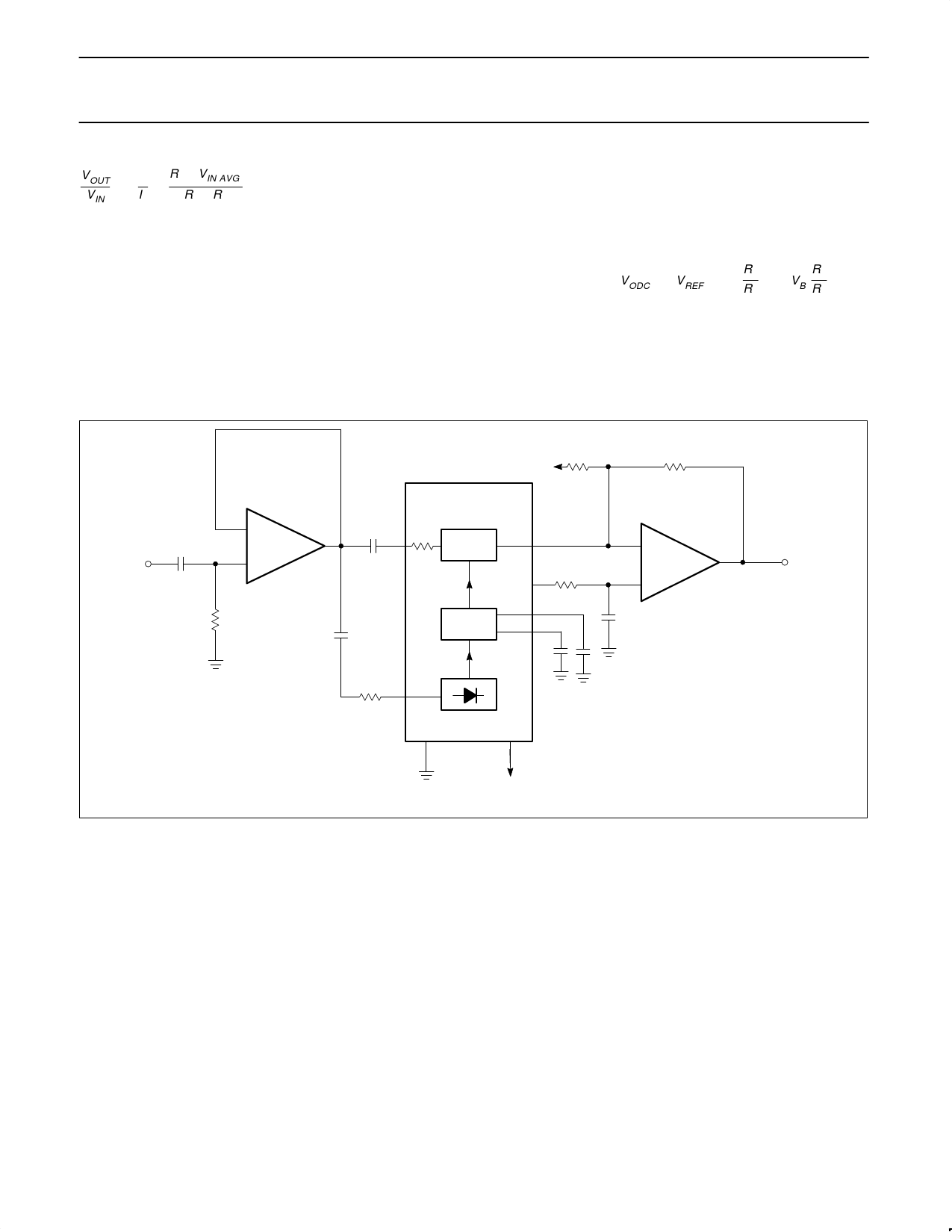
Both the resistors R1 and R2 are tied to
internal summing nodes. R1 is a 6.8k internal
resistor. The maximum input current into the
gain cell can be as large as 140µA. This
corresponds to a voltage level of 140µA •
6.8k=952mV peak. The input peak current
into the rectifier is limited to 300µA by the
internal bias system. Note that the value of
R1 can be increased to accommodate higher
input level. R2 and R3 are external resistors.
It is easy to adjust the ratio of R3/R2 for
desirable system voltage and current levels.
A small R2 results in higher gain control
current and smaller static and dynamic
tracking error. However, an impedance buffer
A1 may be necessary if the input is voltage
drive with large source impedance.
The gain cell output current feeds the
summing node of the external OPA A2. R3
and A2 convert the gain cell output current to
the output voltage. In high-performance
applications, A2 has to be low-noise,
high-speed and wide band so that the
high-performance output of the gain cell will
not be degraded. The non-inverting input of
A2 can be biased at the low noise internal
reference Pin 6 or 10. Resistor R4 is used to
bias up the output DC level of A2 for
maximum swing. The output DC level of A2 is
given by
ǒ Ǔ VODC + VREF 1 )
R3
R4
*
VB
R3
R4
(6)
VB can be tied to a regulated power supply
for a dual supply system and be grounded for
a single supply system. CA sets the attack
time constant and CR sets the recovery time
constant. *5COL
R4
+VB
R3
17.3k
CIN1
VIN
2.2µF
–
A1
+
R5
100k
CIN2
R1
(7,9) 6.8k
CIN3
2.2µF
(5,11)
∆G
VREF
BUFFER
(6,10) R6
1k
(2,14)
(4,12)
A2
C1
2.2µF
R2
3.3k
(3,13)
CA CR
1µF 10µF
(8)
(16)
+VCC
Figure 4. Basic Expandor Schematic
VOUT
October 7, 1987
7
Share Link: 