NJM2519A View Datasheet(PDF) - Japan Radio Corporation
Part Name
Description
Manufacturer
NJM2519A Datasheet PDF : 8 Pages
| |||
NJM2519A
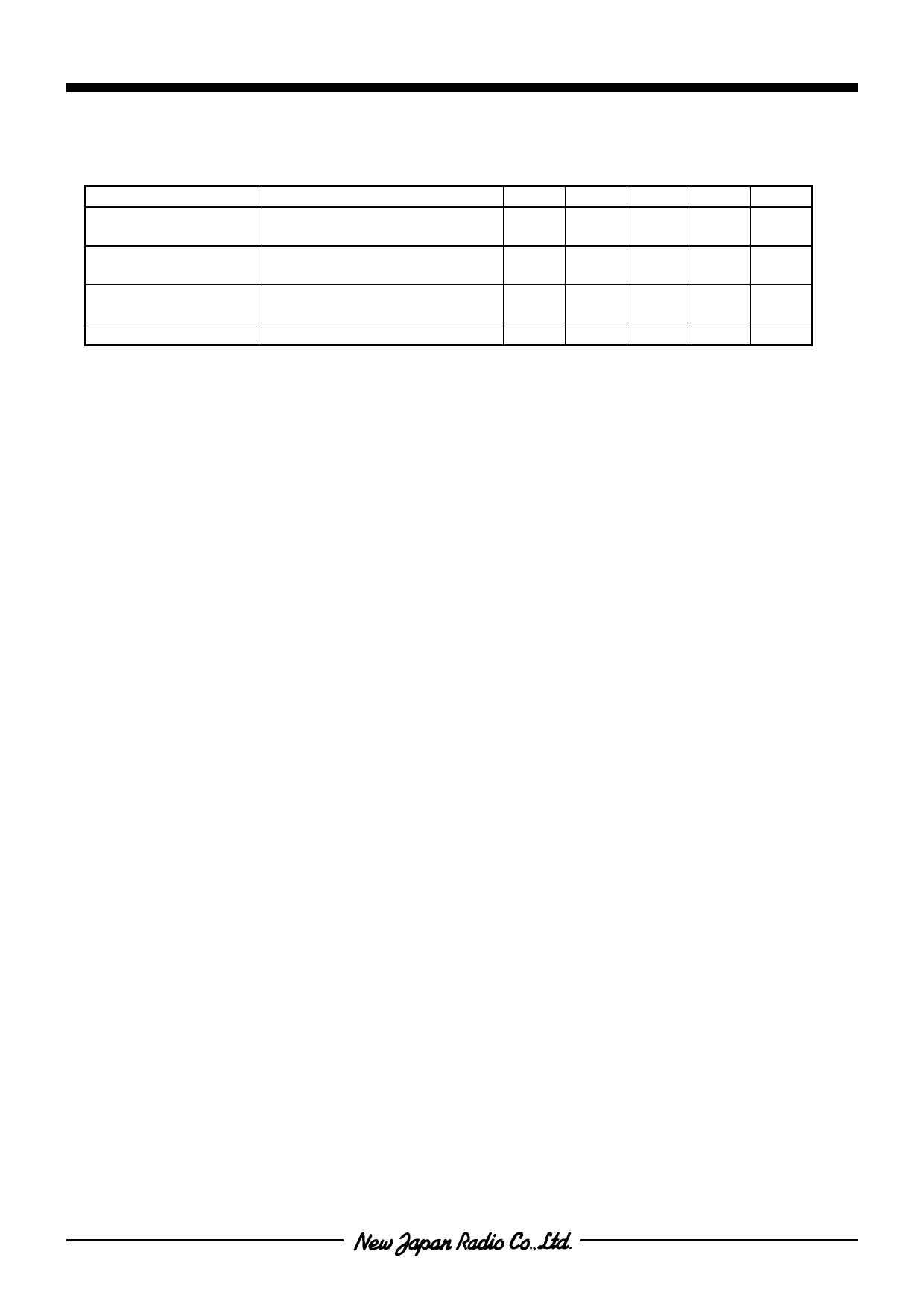
DC ELECTRICAL CHARACTERISTICS (VCC=5V,TA=25°C, otherwise noted. All measurements performed in
the DC test circuit are shown in next page)
Parameter
Condition
(Note 2) Symbol Min. Typ. Max. Unit
Video Output Signal
Amplitude 1
Video Modulation Depth
Video Limiter Modulation
Depth
(Note 2)
Gvv1=Gvvh-Gvvl
Mp=((Gvv-Mw)/Gvv)x100
where Mw=Mwh-Mwl
Mpmax=((Gvv-Wc)/Gvv)x100
where Wc=Wch-Wcl
Gvv 48
Mp
66
Mpmax 85
-
108 mV
-
78
%
94
98
%
Picture-to-sound Ratio Ps=20log(Gvv/(Gva/2))
Ps
8
-
18
dB
(Note 2) Explanation of symbols
• Vv : VIDEO IN output voltage at Pin3
• Voso : OSC output voltage at Pin8
• Gvvh : RF OUT output voltage at Pin1
OSC(Pin8) input = Voso+0.3V
• Gvvl : RF OUT output voltage at Pin1
OSC(Pin8) input = Voso-0.3V
• Mwh : RF OUT output voltage at Pin1
OSC (Pin 8) input = Voso+0.3V,VIDEO IN(Pin3) input=Vv + 0.41V
• Mwl : RF OUT output voltage at Pin1
OSC (Pin 8) input = Voso-0.3V,VIDEO IN(Pin3) input=Vv + 0.41V
• Wch : RF OUT output voltage at Pin1
OSC (Pin 8) input = Voso+0.3V,VIDEO IN(Pin3) input=Vv + 0.75V
• Wcl : RF OUT output voltage at Pin1
OSC (Pin 8) input = Voso-0.3V,VIDEO IN(Pin3) input=Vv + 0.75V
• Gva : RF OUT output level at Pin1(4.5MHz Sine wave [peak to peak])
OSC(Pin8) input = Voso+0.6V
-3-
Share Link: 