NJU6434C View Datasheet(PDF) - Japan Radio Corporation
Part Name
Description
Manufacturer
NJU6434C Datasheet PDF : 14 Pages
| |||
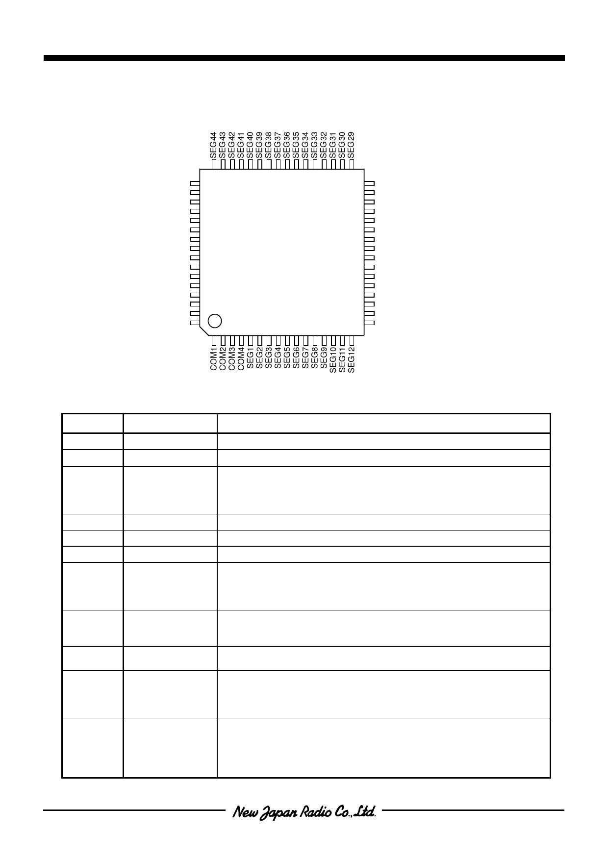
! PIN CONFIGURATION
NJU6434
SEG45
SEG46
SEG47
SEG48
SEG49
SEG50
VLCD
INHb
SCL
DATA
CE
MODE
VSS
OSC1
OSC2
VDD
NJU6434
SEG28
SEG27
SEG26
SEG25
SEG24
SEG23
SEG22
SEG21
SEG20
SEG19
SEG18
SEG17
SEG16
SEG15
SEG14
SEG13
! TERMINAL DESCRIPTION
No.
5~54
1~4
SYMBOL
SEG1~SEG50
COM1~COM4
62
OSC1
63
OSC2
64
VDD
61
VSS
55
VLCD
59
CE
57
SCL
58
DATA
60
MODE
56
INHb
FUNCTION
LCD Segment Output Terminals
LCD Common Output Terminals
Oscillation Terminals :
External resistance is connected to these terminals.
In External clock operation, the external clock input to OSC1
terminal. OSC2 terminal should be opened.
Power Supply (+5V)
Power Supply (0V)
Power Supply for LCD Driving
Chip Enable Signal Input Terminal :
"H" : LCD display data and mode setting data input
"L" : Disable
Fall Edge : LCD display data latch
Serial Data Transmission Clock Input Terminal :
LCD display and Mode setting data are input synchronized
SCL clock signal rise edge.
Serial Data Input Terminal
Data input timing : SCL clock rise edge
Data or Mode Select Terminal
"H" : Data input mode
"L" : LCD display data input mode
(Refer the mode setting table for mode setting contents)
Display-Off Control Terminal :
When display goes to off, the display data in the shift-register is
retained.
"H" : Display-On
"L" : Display-Off
Ver.2009-11-12
-3-
Share Link: 