NJU6538 View Datasheet(PDF) - Japan Radio Corporation
Part Name
Description
Manufacturer
NJU6538 Datasheet PDF : 27 Pages
| |||
NJU6538
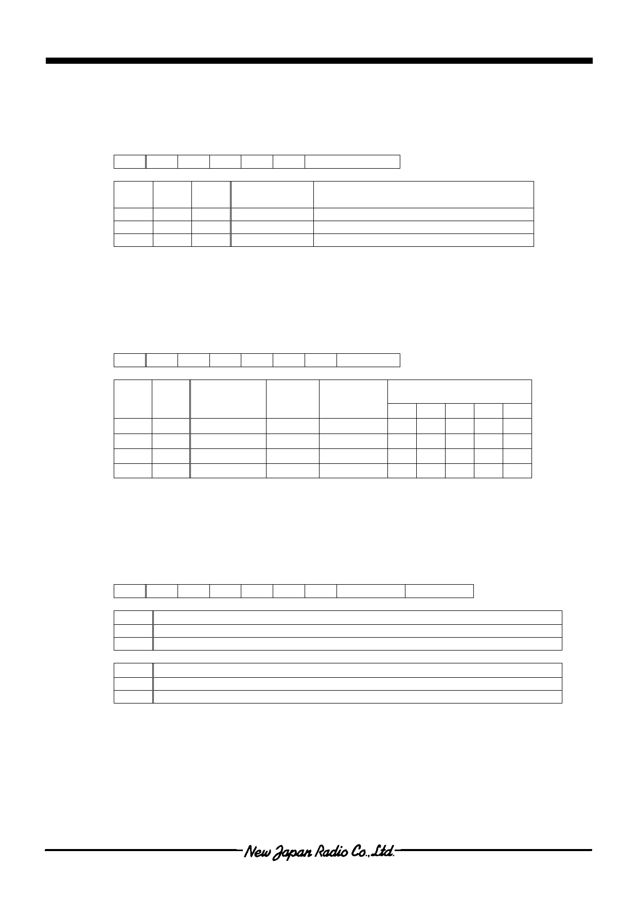
(j) Duty select
Duty select instruction is which sets LCD driving duty ratio 1/8 or 1/9 or 1/10 duty.
A0 D7 D6 D5 D4 D3 D2 D1 D0
000110
Duty
D2
D1
D0
0
0
0
0
0
1
0
1
0
Duty ratio
1/8 Duty
1/9 Duty
1/10 Duty
Scan Common
COM1 to COM8 (5x7 character + 1-icon )
COM1 to COM9 (5x7 character + 2-icon )
COM1 to COM10 (5x7 character + 3-icon )
(k) Power save mode set
Power save mode reduces the operating current of application using Display Off and selects a
terminal condition of Key scan signal output. The terminal, which is set to "L", does not output Key
scan signal as shown in following table.
A0 D7 D6 D5 D4 D3 D2 D1 D0
0
0
1
0
0
0
0
Power save
D1
D0
Function
0
0
Normal
0
1 Power save 1
1
0 Power save 2
1
1 Power save 3
*1 No scanning states.
Internal
OSC.
ON
Stop
Stop
Stop
LCD output
ON
Display Off
Display Off
Display Off
Key scanning output terminals
states *1
S0 S1 S2 S3 S4
HHHHH
L L L LH
L L LHH
HHHHH
(l) General output port PWM phase / freqency set
General output port PWM phase / frequency set instruction setting PWM phase and PWM
frequency.
A0 D7 D6 D5 D4 D3 D2
0010100
D1
Phase
D0
Frequency
D1
General Output Port PWM phase set
0 32-steps shift phase PWM output timinng by Po0 to Po1, Po1 to Po2, Po2 to Po3.
1 same phase PWM output timinng by Po0 to Po3.
D0
General Output Port PWM frequency set
0 fsys / 128 frequency. (Default)
1 fsys / 256 frequency.
(fsys : system clock = fosc / 2)
- 10 -
Ver.2003-05-09
Share Link: 