NJU6538 View Datasheet(PDF) - Japan Radio Corporation
Part Name
Description
Manufacturer
NJU6538 Datasheet PDF : 27 Pages
| |||
NJU6538
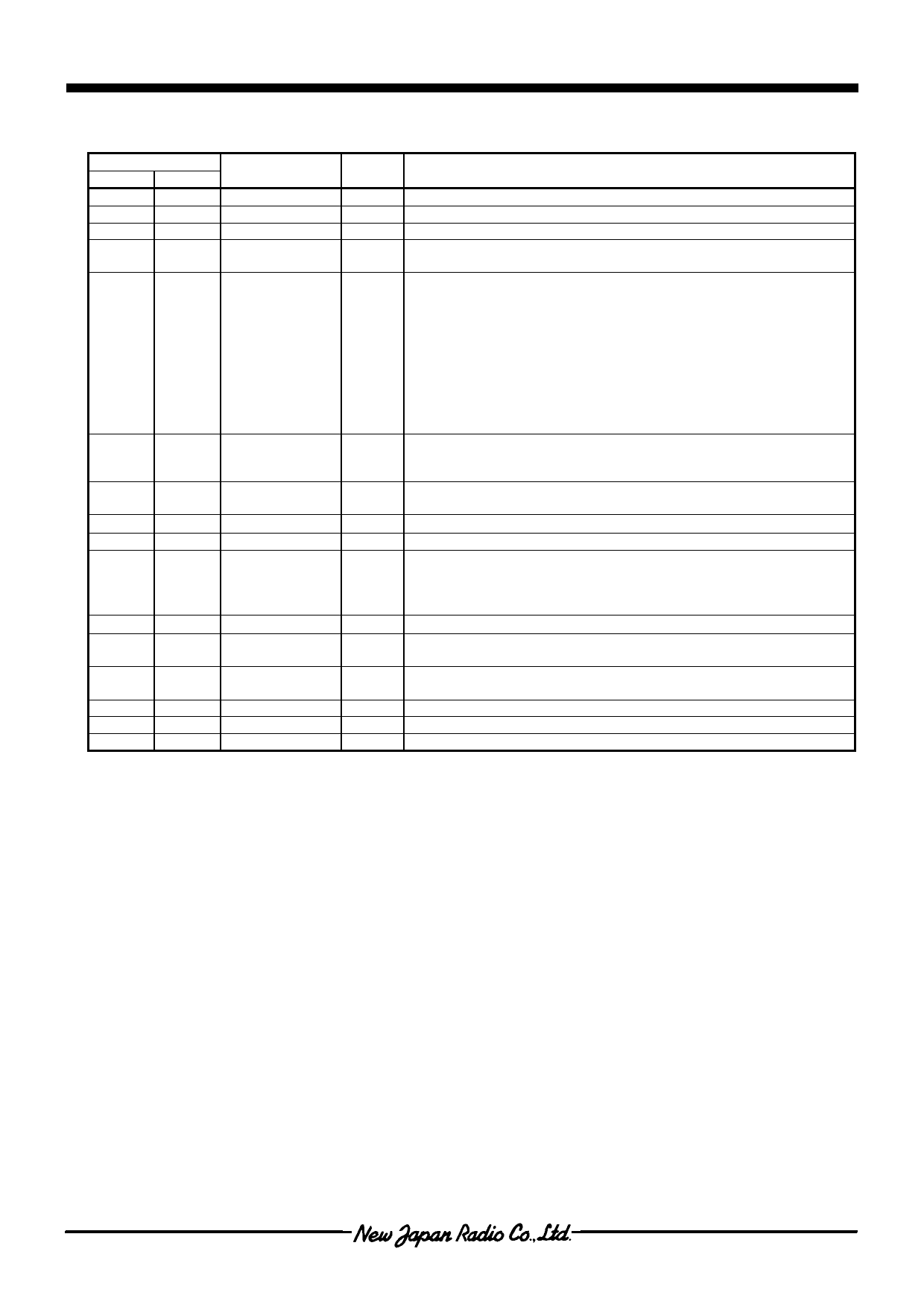
TERMINAL DESCRIPTION
No.
FG1
FC2
1 to 65 3 to 67
66 to 72 68 to 74
73 to 75 75 to 77
76 to 78 78 to 80
Symbol
SEG1 to SEG65
COM1 to COM7
COM8 to COM10
Po0 to Po2
79
81
Po3/S0
I/O
Description
O Segment output terminal.
O Common output terminal.
O Icon common output terminal.
O
General output port
128-step PWM waveform output by MPU control.
General output port / Key scanning input terminal
Select General output port or Key scanning input terminal by the
instruction.
A function must be selected either Po3 or S0
O
General output port
128-step PWM waveform output by MPU control.
80 to 83 82 to 85
84 to 88 86 to 90
89
91
90
92
91
93
92
94
93
94
94
96
95
97
96
98
97
99
98
100
99
1
100
2
S1 to S4
K0 to K4
VDD
VLCD1
VLCD2
V0
V1
V2
VSS
OSC
RESb
CE
SCL
SIO
Key scanning input terminals
(No need for anti-reverse current diode in key scan)
O
Key scanning input terminals.
(No need for anti-reverse current diode in key scan)
I
Key scanning input terminals.
(with internal pull-down resistor)
- Power supply terminal.(2.7V to 5.5V)
I
LCD driving voltage input terminal.
I
LCD driving voltage stabilization capacitor terminals.
Connect the capacitor between each terminal and Vss.
- Ground terminal.
I/O
Osclator terminal.
Conect the external resistor.
I
Reset terminal. (with internal pull-up resistor)
In case of only Power-on Reset should be open.
I
Chip enable terminal
I
Serial clock input terminal
I/O Serial Data input or output terminal
-4-
Ver.2003-05-09
Share Link: 