NJU6538 View Datasheet(PDF) - Japan Radio Corporation
Part Name
Description
Manufacturer
NJU6538 Datasheet PDF : 27 Pages
| |||
NJU6538
(2) Instruction
3-wired Serial I/F is clock synchronized of the SCL clock. and D7 to D0 signal select data or instruction by
A0 signal.
The data input as MSB(D7) first serially.
Instruction
(a) Display ON/OFF
(b) Page address set
Culumn address set
Higher order 3-bits
(c)
Culumn address set
Lower order 4-bits
(d) Display data write
(e) ADC select
(f) Inverse display On / Off
Whole display ON
(g) / Normal display
(h) Reset
(i) E.V.R. Register Set
(j) Duty select
(k) Power save mode set
General output port
(l) PWM phase / freqency set
General output port serect
General output port PWM set
(m) High order 3-bits
/ PWM enable set
General output port PWM set
Lower order 4-bits
General output port /
(n)
Key scan output select
(o) Maker test
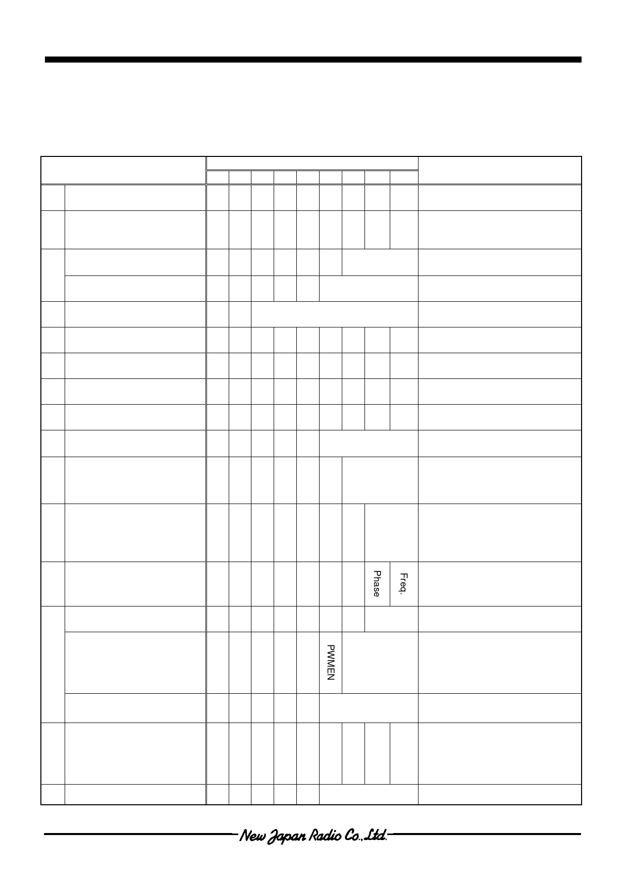
Table 1. Instruction Code
(*: Don’t Care)
Code
A0 D7 D6 D5 D4 D3 D2 D1 D0
Description
LCD display ON / OFF
0 1 0 1 0 1 1 1 0/1
D0=0 : OFF, D0=1 : ON
Set the page of DDRAM to the page
0 1 0 1 1 0 0 0 0/1 address registor.
00001 *
Higher order
Column add.
D0=0 : PAGE 0, D0=1 : PAGE 1
Set the Higher order 3 bits column
address to rhe registor.
00000
Lower order
Column add.
Set the Lower order 4 bits column
address to rhe registor.
1*
Write data
Write the data into the Display data
RAM(DDRAM)
Set the DDRAM to SEG driver
0 1 0 1 0 0 0 0 0/1
D0=0 : Nomal, D0=1 : Inverse
Inverse LCD display ON / OFF
0 1 0 1 0 0 1 1 0/1
D0=0 : Nomal, D0=1 : Inverse
Whole Display tern ON
0 1 0 1 0 0 1 0 0/1
D0=0: Normal, D0=1: Whole Display
0 1 1 1 0 0 0 1 0 Initialize the internal circuit
00010
E.V.R. data
Set the Contrast control E.V.R.
(16 steps)
Duty set (1/8,1/9,1/10)
000110
Duty
(D2,D1,D0)=( 0,0,0) : 1/8Duty
(D2,D1,D0)=( 0,0,1) : 1/9 Duty
(D2,D1,D0)=( 0,1,0) : 1/10 Duty
Set the Power save mode
0010000
Power
save
(D1,D0)=(0,0) : Nomal
(D1,D0)=(0,1) : Power save 1
(D1,D0)=(1,0) : Power save 2
(D1,D0)=(1,1) : Power save 3
0010100
Set the PWM phase / freqency
D1: PWM Phase set
D0: PWM Freqenccy set
0011000
Select the General output port for
Port
PWM level set
01000
High order
PWM data
PWMEN=0:”L” output
PWMEN=1:PWM output
Set the Higher order 3 bits PWM
data to rhe registor.
00111
Lower order
PWM data
Set the Lower order 4 bits PWM
data to rhe registor.
Select General output port or Key
scan output select by Po3/S0
0 1 0 0 1 0 0 0 0/1 terminal
D0=0 : General output port
D0=1 : Key scan output
01111
Test data
Do not use this instruction.
-6-
Ver.2003-05-09
Share Link: 