NT6868A View Datasheet(PDF) - Unspecified
Part Name
Description
Manufacturer
NT6868A Datasheet PDF : 14 Pages
| |||
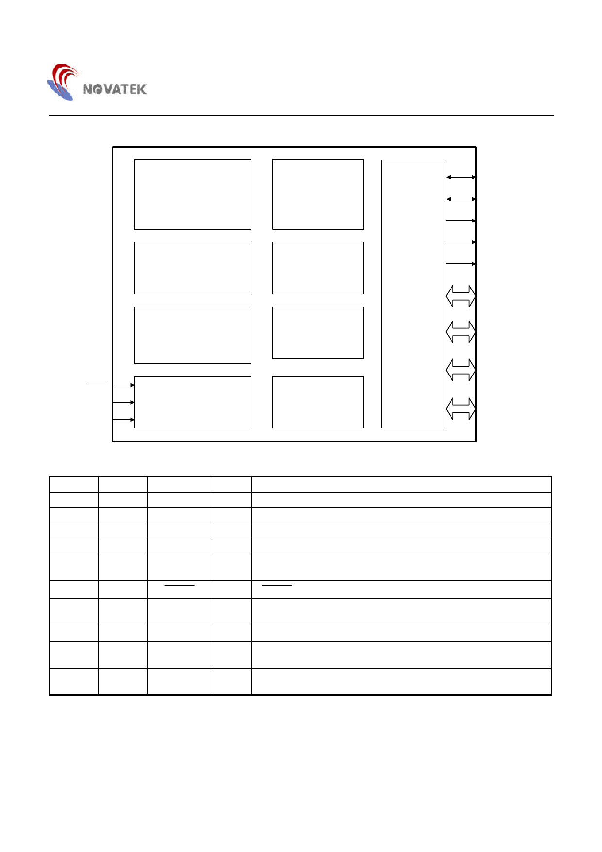
Block Diagram
NT6868A
TIMING GENERATOR
(RC OSC/CERAMIC RESONATOR:
4MHz)
6502
CPU
RESET
VDD
GND
INT. CONTROLLER
POWER-ON RESET/
LOW VOLTAGE RESET
4K BYTES
ROM
128 BYTES
SRAM + STACK
WATCH DOG
TIMER
BASE TIMER
I/O PORTS
CLK
DATA
LED0
LED1
LED2
P00 - P07
P10 - P17
P20 - P27
P30 - P34
Pin and Pad Descriptions
Pin No. Pad No. Designation I/O
1
1
GND
P
2
2
NC
-
3
3
DATA
I/O
4
4
CLK
I/O
5 - 9,
5 - 9,
P30 - P34,
I/O
11 - 34 11 - 34 P00 - P27
10
10
RESET
I
35 - 37 35 - 37
LED0 -
O
LED2
38
38
VDD
P
39
39
R/OSCO
I
40
40
OSCI
-
Description
Ground pin
No connection, recommended to connect VDD or floating
I/O, 10KΩ pull-up resistor for communication
I/O, 10KΩ pull-up resistor for communication
Bi-directional I/O pins
RESET signal input pin with internal pull up resistor; Active low
LED direct sink pins
Power supply
47KΩ resistor connected for RC OSC or 4MHz ceramic resonator
connected
No connection for RC OSC, connected for 4MHz ceramic
resonator
* Under the constraint of the maximum frequency variation, (∆F/F)max, ≤ ±1%, code 3 (ceramic resonator option) must be
selected and pin 39 and pin 40 are connected to a ceramic resonator. If (∆F/F)max, ≤ ±10%, code 1 (RC OSC option) is
recommended to be selected and pin39 connects a 47KΩ resistor with, ≤ ±1% accuracy to VDD and pin 40 is floating.
2
Share Link: 