NTE1567 View Datasheet(PDF) - NTE Electronics
Part Name
Description
Manufacturer
NTE1567 Datasheet PDF : 4 Pages
| |||
General Description:
Output Stage and Protection Circuit
Pin5 is the output pin. The supply for the output stage is fed to Pin6 and the output stage is fed to
Pin6 and the output stage ground is connected to Pin4. The output transistors of the class−B output
stage can each deliver 1A maximum. The upper power transistor is protected against short−circuit
currents to ground, whereas, during flyback, the “lower” power transistor is protected against short−
circuit currents to ground, whereas, during flyback, the “lower” power transistor is protected against
too high voltages which may occur during adjustments.
Moreover, the output transistors have been given extra solidity by means of special measures in the
internal circuit layout.
A thermal protection circuit is incorporated to protect the IC against too high dissipation. This circuit
is “active” at 175°C and then reduces the deflection current to such as value that the dissipation can-
not increase.
Driver and Switching Circuit:
Pin1 is the input for the driver of the output stage. The signal at Pin1 is alos applied to Pin3 which
is the input of a switching circuit. When the flyback starts, this switching circuit rapidly turns off the
lower output stage and so limits the turn−off dissipation. It also allows a quick start of the flyback gen-
erator. Pin3 is connected externally to Pin1, in order to allow for different applications in which Pin3
is driven separate from Pin1.
Flyback Generator
The capacitor at Pin6 is charged to a maximum voltage, which is equal to the supply voltage Vp (Pin9),
during scan.
When the flyback starts and the voltage at the output pin (Pin5) exceeds the supply voltage (Pin9),
the flyback generator is activated. The Vp is connected in series (via Pin8) with the voltage across
the capacitor.
The voltage at the supply pin (Pin6) of the output stage will then be maximum twice Vp. Lower volt-
ages can be chosen by changing the value of the external resistor at Pin8.
Voltage Stabilizer
The internal voltage stabilizer provides a stabilized supply of 6V for drive of the output stage, so the
drive current of the output stage is not affected by supply voltage variations. The stabilized voltage
is available at Pin7.
A decoupling capacitor of 2.2µF can be connected to this pin.
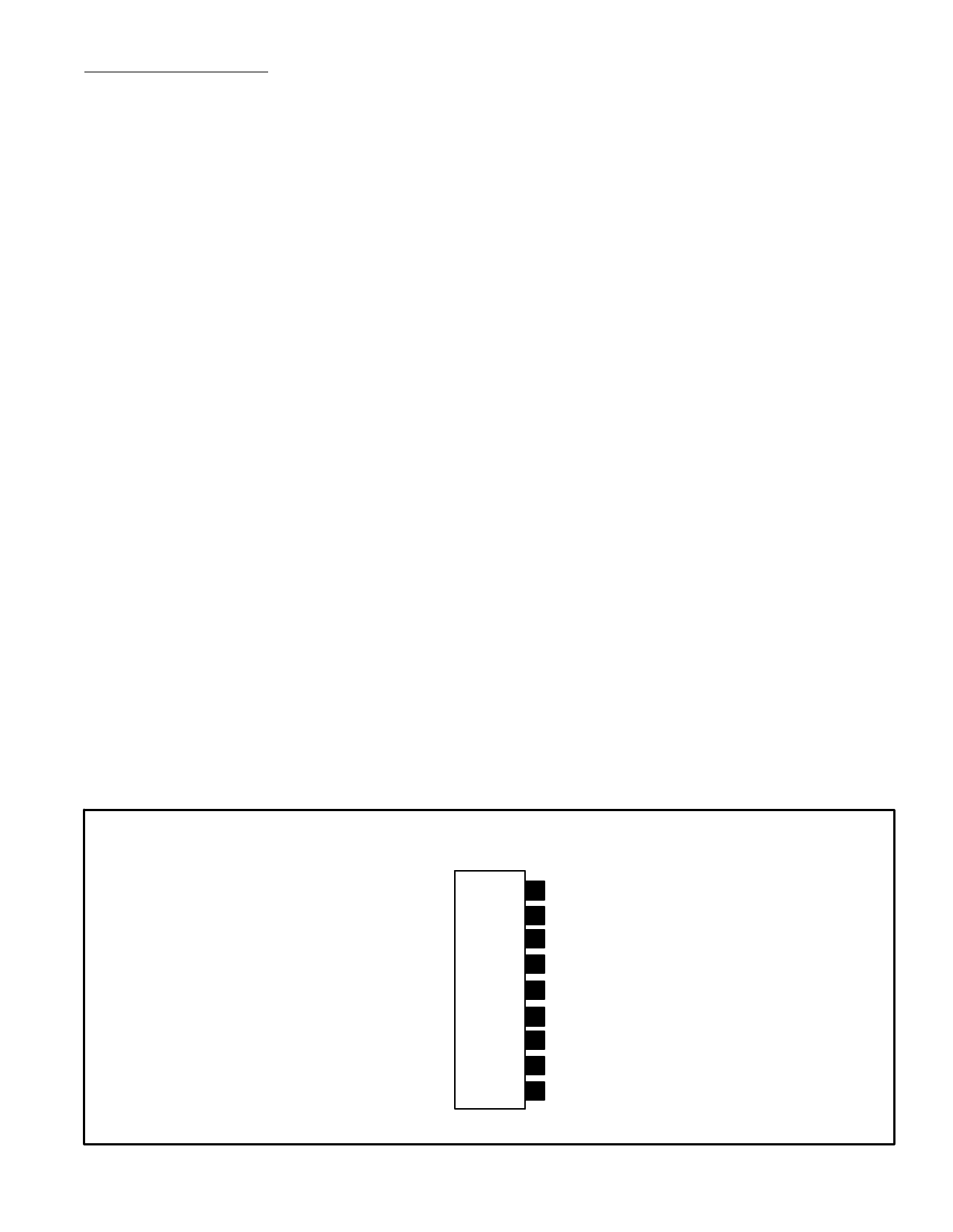
Pin Connection Diagram
(Front View)
9 VCC
8 Flyback Input
7 Blank Output
6 Output VCC
5 Output
4 Output (GND)
3
Switching Circuit
Input
2 GND
1 Driver Input
Share Link: 