NTE1857 View Datasheet(PDF) - NTE Electronics
Part Name
Description
Manufacturer
NTE1857 Datasheet PDF : 6 Pages
| |||
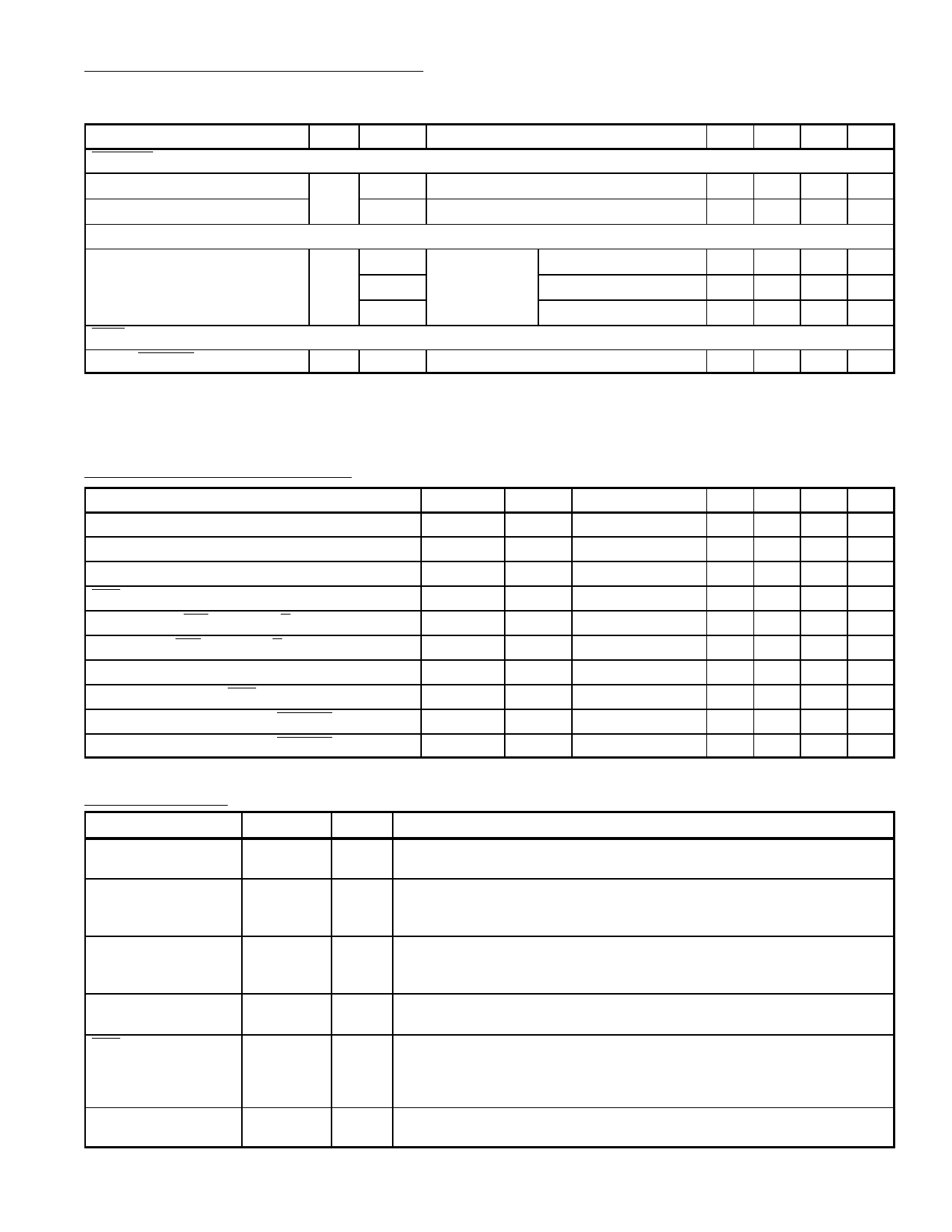
DC Electrical Characteristics (Cont’d): (Specifications apply over the recommended supply
voltage and temperature ranges unless otherwise spe–
cified, See Notes 2, 3)
Parameter
Pins Symbol
Test Conditions
Min Typ Max Unit
Phase A Output
Output Low Voltage
Off State Leakage Current
Power Supply
11 VOLA IOA = 8mA
IOHA VOHA = 16.5V
– – 0.4 V
– – 100 µA
Power Supply Current
Bias/Set Current
16
IMW IOD = 0µA,
L3 = VOHD, L4 = VOLD –
– 70 mA
IMZ
IBS = –300µA,
L1 = VOHD,
L3 = HiZ, L4 = HiZ
– – 40 mA
IMN L2 = VOLD
L3 = VOHD, L4 = VOLD –
– 75 mA
To Set Phase A
6
IBS
–5.0 – – µA
Note 2. Algebraic convention rather than absolute values is used to designate limit values.
Note 3. Current into a pin is designated as positive. Current out of a pin is designated as negative.
AC Switching Characteristics: (TA = +25°C, VM = 12V unless otherwise specified)
Parameter
Pins Symbol Test Conditions Min Typ Max Unit
Clock Frequency
Clock Pulse Width – High
Clock Pulse Width – Low
Bias/Set Pulse Width
Setup Time – CW/CCW and F/HS
Hold Time – CW/CCW and F/HS
Propagation Delay – Clk–to–Driver Output
Propagation Delay – Bias/Set–to–Driver Output
Propagation Delay – Clk–to–Phase A Low
Propagation Delay – Clk–to–Phase A High
7
7
7
6
10–7, 9–7
10–7, 9–7
7–11
7–11
fCK
PWCKH
PWCKL
PWBS
tsu
th
tPCD
tPBSD
tPHLA
tPLHA
0 – 50 kHz
10 – – µs
10 – – µs
10 – – µs
5 – – µs
10 – – µs
– 8 – µs
– 1 – µs
– 12 – µs
– 5 – µs
Pin Description:
Name
Power Supply
Ground
Clamp Diode
Voltage
Driver Outputs
Bias/Set
Clock
Symbol
VM
GND
VD
L1, L2,
L3, L4
B/S
Clk
Pin #
16
4, 5,
12, 13
1
2, 3,
14, 15
6
7
Description
Power supply pin for both the logic circuit and the motor coil current. Volt-
age is +7.2 to +16.5V.
Ground pins for the logic circuit and the motor coil current. The physical
configuration of the pins aids in dissipating heat from within the IC pack-
age.
This pin is used to protect the outputs where large voltage spikes may oc-
cur as the motor coils are switched. Typically a diode is connected be-
tween this pin and Pin16.
High current outputs for the motor coils. L1 and L2 are connected to one
coil, and L3 and L4 to the other coil.
This pin is typically 0.7 below VM. The current out of this pin (through a
resistor to GND) determines the maximum output sink current. If the pin
is opened (IBS < 5.0µA) the outputs assume a high impedance condition,
while the internal logic presets to a Phase A condition.
The positive edge of the clock input switches the outputs to the next posi-
tion. This input has no effect if Pin6 is open.
Share Link: 