P80CE598FFB View Datasheet(PDF) - Philips Electronics
Part Name
Description
Manufacturer
P80CE598FFB Datasheet PDF : 108 Pages
| |||
Philips Semiconductors
8-bit microcontroller with on-chip CAN
Product specification
P8xCE598
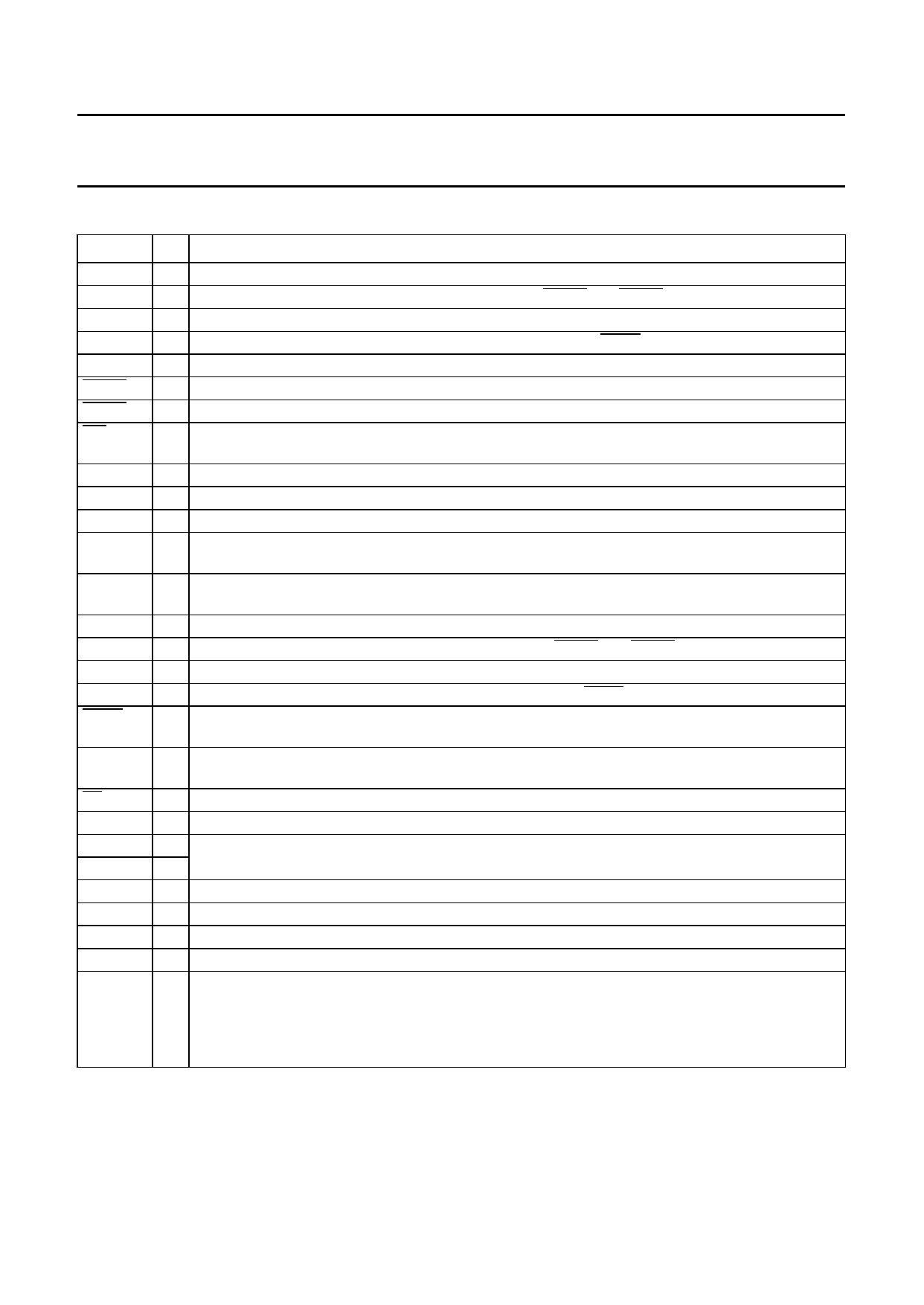
Table 1 Pin description for single function pins (SOT318-1 and SOT351-1; see note 1)
SYMBOL PIN
DESCRIPTION
VDD1
VDD2
VDD3
VDD4
STADC
14 Power supply, digital part: for internal logic (CPU, Timers/counters, Memory, CAN, UART, ADC).
28 Power supply, digital part: for Port 1, Port 3, Port 4, PWM0 and PWM1 outputs.
53 Power supply, digital part: for the on-chip oscillator.
76 Power supply, digital part: for Port 0, Port 2, ALE output and PSEN output.
15 Start ADC operation. Input starting analog-to-digital conversion (note 2). This pin must not float.
PWM0 16 Pulse width modulation output 0.
PMW1 17 Pulse width modulation output 1.
EW
18 Enable Watchdog Timer (WDT): enable for T3 Watchdog Timer and disable Power-down mode.
This pin must not float.
RST
30 Reset: input to reset the P8xCE598 (note 3).
CVSS
CVDD
XTAL2
37 Ground potential for the CAN transmitter outputs.
40 Power supply (+5V) for the CAN transmitter outputs.
51 Crystal pin 2: output of the inverting amplifier that forms the oscillator.
When an external clock oscillator is used this pin is left open-circuit.
XTAL1
52 Crystal pin 1: input to the inverting amplifier that forms the oscillator, and input to the internal clock
generator. Receives the external clock oscillator signal, when an external oscillator is used.
VSS1
VSS2
VSS3
VSS4
PSEN
13 Ground, digital part: for internal logic (CPU, Timers/Counters, Memory, CAN, UART, ADC).
29 Ground, digital part: for Port 1, Port 3 and Port 4, and PWM0 and PWM1 outputs.
54 Ground, digital part: for the on-chip oscillator.
77 Ground, digital part: for the Port 0, Port 2, ALE output and PSEN output.
63 Program Store Enable: Read strobe to external Program Memory (active LOW).
Drive: 8 × LSTTL inputs.
ALE
64 Address Latch Enable: latches the Low-byte of the address during accesses to external memory
(note 4). Drive: 8 × LSTTL inputs; handles CMOS inputs without an external pull-up.
EA
REF
CRX1
CRX0
65 External Access input. See note 5.
78 1⁄2AVDD reference voltage output respectively input (note 6).
79 Inputs from the CAN-bus line to the differential input comparator of the on-chip CAN-controller
80 (note 7).
AVREF−
AVREF+
AVSS
AVDD
n.c.
1 Low-end of ADC (analog-to-digital conversion) reference resistor.
2 High-end of ADC (analog-to-digital conversion) reference resistor (note 8).
3 Ground, analog part. For ADC, CAN receiver and reference voltage.
4 Power supply, analog part (+5 V). For ADC, CAN receiver and reference voltage.
23, No connection.
49,
50,
66,
67
Notes
1. To avoid a ‘latch up’ effect at power-on: VSS − 0.5 V < ‘voltage on any pin at any time’ < VDD + 0.5 V.
2. Triggered by a rising edge. ADC operation can also be started by software.
3. RST also provides a reset pulse as output when timer T3 overflows or after a CAN wake-up from Power-down.
1996 Jun 27
8
Share Link: 