P89LPC920 View Datasheet(PDF) - Philips Electronics
Part Name
Description
Manufacturer
P89LPC920
Philips Electronics

P89LPC920 Datasheet PDF : 45 Pages
| |||
Philips Semiconductors
P89LPC920/921/922
8-bit microcontrollers with two-clock 80C51 core
Table 3: Pin description…continued
Symbol
Pin
Type Description
P3.0 - P3.1 7, 6
I/O Port 3: Port 3 is an 2-bit I/O port with a user-configurable output type. During reset
Port 3 latches are configured in the input only mode with the internal pull-up disabled.
The operation of Port 3 pins as inputs and outputs depends upon the port configuration
selected. Each port pin is configured independently. Refer to Section 8.12.1 “Port
configurations” and Table 8 “DC electrical characteristics” for details.
All pins have Schmitt triggered inputs.
Port 3 also provides various special functions as described below:
7
I/O P3.0 — Port 3 bit 0.
O
XTAL2 — Output from the oscillator amplifier (when a crystal oscillator option is
selected via the FLASH configuration.
O
CLKOUT — CPU clock divided by 2 when enabled via SFR bit (ENCLK - TRIM.6). It
can be used if the CPU clock is the internal RC oscillator, watchdog oscillator or
external clock input, except when XTAL1/XTAL2 are used to generate clock source for
the real time clock/system timer.
6
I/O P3.1 — Port 3 bit 1.
I
XTAL1 — Input to the oscillator circuit and internal clock generator circuits (when
selected via the FLASH configuration). It can be a port pin if internal RC oscillator or
watchdog oscillator is used as the CPU clock source, and if XTAL1/XTAL2 are not used
to generate the clock for the real time clock/system timer.
VSS
5
I
Ground: 0 V reference.
VDD
15
I
Power Supply: This is the power supply voltage for normal operation as well as Idle
and Power Down modes.
[1] Input/Output for P1.0-P1.4, P1.6, P1.7. Input for P1.5.
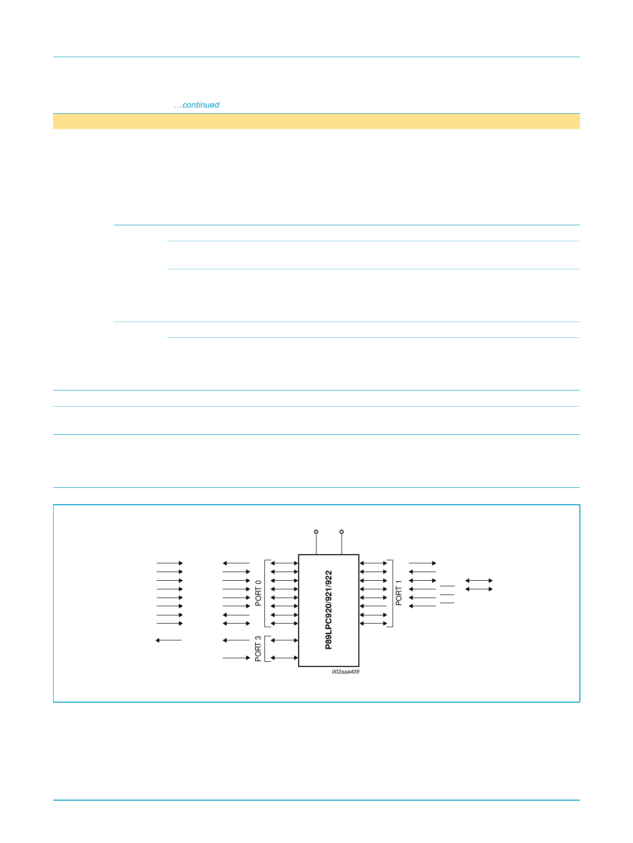
6. Logic symbol
KBI0
KBI1
KBI2
KBI3
KBI4
KBI5
KBI6
KBI7
CLKOUT
Fig 4. Logic symbol.
CMP2
CIN2B
CIN2A
CIN1B
CIN1A
CMPREF
CMP1
T1
XTAL2
XTAL1
VDD VSS
002aaa409
TxD
RxD
T0
INT0
INT1
RST
SCL
SDA
9397 750 12285
Product data
Rev. 06 — 21 November 2003
© Koninklijke Philips Electronics N.V. 2003. All rights reserved.
8 of 45
Share Link: