P89C660 View Datasheet(PDF) - Philips Electronics
Part Name
Description
Manufacturer
P89C660 Datasheet PDF : 89 Pages
| |||
Philips Semiconductors
80C51 8-bit Flash microcontroller family
16KB/32KB/64KB ISP/IAP Flash with 512B/1KB/2KB/8KB RAM
Product data
P89C660/P89C662/P89C664/
P89C668
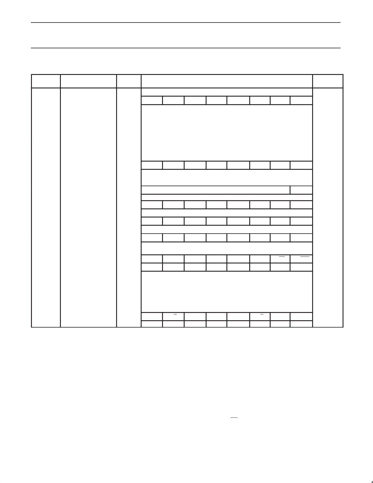
Table 1 Special Function Registers (Continued)
SYMBOL
DESCRIPTION
DIRECT
BIT ADDRESS, SYMBOL, OR ALTERNATIVE PORT FUNCTION
ADDRESS MSB
LSB
D7
D6
D5
D4
D3
D2
D1
D0
PSW*
Program Status Word
D0H
CY
AC
F0
RS1 RS0
OV
F1
P
RCAP2H#
RCAP2L#
Timer 2 Capture High
Timer 2 Capture Low
CBH
CAH
SADDR# Slave Address
A9H
SADEN# Slave Address Mask
B9H
RESET
VALUE
00000000B
00H
00H
00H
00H
S0BUF
Serial Data Buffer
S0CON*
SP
S1DAT#
S1ADR#
Serial Control
Stack Pointer
Serial 1 Data
Serial 1 Address
99H
9F
9E
9D
9C
9B
9A
99
98H SM0/FE SM1 SM2 REN
TB8
RB8
TI
81H
DAH
DBH
SLAVE ADDRESS
xxxxxxxxB
98
RI 00H
07H
00H
GC 00H
S1STA# Serial 1 Status
S1CON*# Serial 1 Control
TCON*
Timer Control
D9H
D8H
88H
SC4 SC3 SC2 SC1 SC0
DF
DE
DD
DC
DB
CR2 ENS1 STA STO
SI
8F
8E
8D
8C
8B
TF1
TR1
TF0 TR0
IE1
0
0
0
F8H
DA
D9
D8
AA CR1 CR0 00000000B
8A
89
88
IT1
IE0
IT0 00H
CF
CE
CD
CC
CB
CA
C9
C8
T2CON* Timer 2 Control
C8H
TF2 EXF2 RCLK TCLK EXEN2 TR2 C/T2 CP/RL2 00H
T2MOD# Timer 2 Mode Control
C9H
–
–
–
–
–
– T2OE DCEN xxxxxx00B
TH0
Timer High 0
8CH
00H
TH1
Timer High 1
8DH
00H
TH2#
Timer High 2
CDH
00H
TL0
Timer Low 0
8AH
00H
TL1
Timer Low 1
8BH
00H
TL2#
Timer Low 2
CCH
00H
TMOD
Timer Mode
89H GATE C/T
M1
M0
GATE C/T
M1
M0 00H
WDTRST Watchdog Timer Reset A6H
* SFRs are bit addressable.
# SFRs are modified from or added to the 80C51 SFRs.
– Reserved bits.
OSCILLATOR CHARACTERISTICS
XTAL1 and XTAL2 are the input and output, respectively, of an
inverting amplifier. The pins can be configured for use as an
on-chip oscillator.
To drive the device from an external clock source, XTAL1 should be
driven while XTAL2 is left unconnected. Minimum and maximum
high and low times specified in the data sheet must be observed.
This device is configured at the factory to operate using 6 clock
periods per machine cycle, referred to in this datasheet as “6 clock
mode”. (This yields performance equivalent to twice that of standard
80C51 family devices). It may be optionally configured on
commercially-available EPROM programming equipment to operate
at 12 clock periods per machine cycle, referred to in this datasheet
as “12 clock mode”. Once 12 clock mode has been configured, it
cannot be changed back to 6 clock mode.
RESET
A reset is accomplished by holding the RST pin high for at least two
machine cycles (12 oscillator periods in 6 clock mode, or 24
oscillator periods in 12 clock mode), while the oscillator is running.
To insure a good power-on reset, the RST pin must be high long
enough to allow the oscillator time to start up (normally a few
milliseconds) plus two machine cycles. At power-on, the voltage on
VCC and RST must come up at the same time for a proper start-up.
Ports 1, 2, and 3 will asynchronously be driven to their reset
condition when a voltage above VIH1 (min.) is applied to RST.
The value on the EA pin is latched when RST is deasserted and has
no further effect.
2002 Oct 28
10
Share Link: 