P89C660 View Datasheet(PDF) - Philips Electronics
Part Name
Description
Manufacturer
P89C660 Datasheet PDF : 89 Pages
| |||
Philips Semiconductors
80C51 8-bit Flash microcontroller family
16KB/32KB/64KB ISP/IAP Flash with 512B/1KB/2KB/8KB RAM
Product data
P89C660/P89C662/P89C664/
P89C668
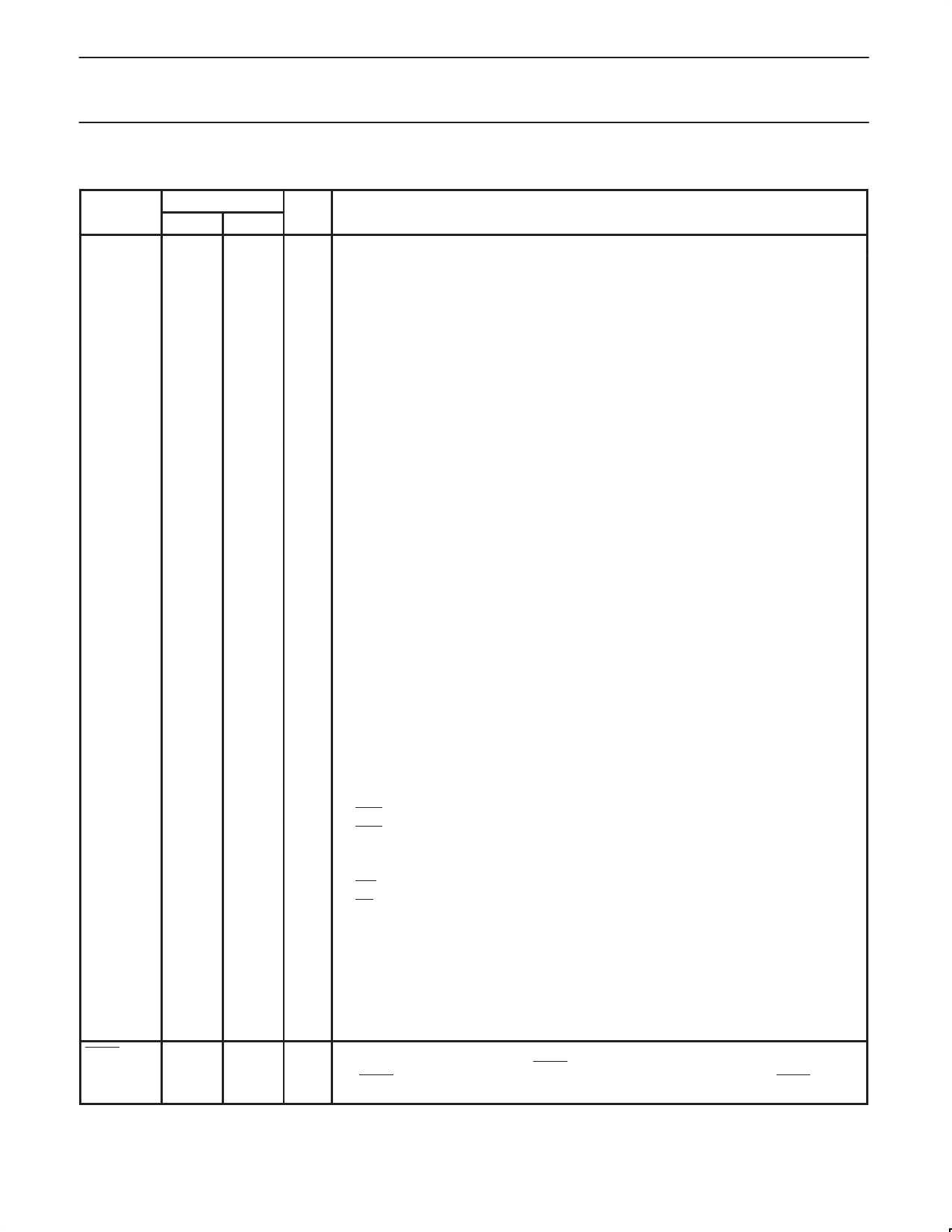
PIN DESCRIPTIONS
PIN NUMBER
MNEMONIC
PLCC LQFP
VSS
VCC
P0.0–0.7
22
44
43–36
16
38
37–30
P1.0–P1.7
2–9 40–44,
1–3
P2.0–P2.7
2
3
4
5
6
7
8
9
24–31
40
41
42
43
44
1
2
3
18–25
P3.0–P3.7
11,
5, 7–13
13–19
RST
ALE
11
5
13
7
14
8
15
9
16
10
17
11
18
12
19
13
10
4
33
27
PSEN
32
26
TYPE
NAME AND FUNCTION
I Ground: 0 V reference.
I Power Supply: This is the power supply voltage for normal, idle, and power-down operation.
I/O Port 0: Port 0 is an open-drain, bidirectional I/O port. Port 0 pins that have 1s written to them
float and can be used as high-impedance inputs. Port 0 is also the multiplexed low-order
address and data bus during accesses to external program and data memory. In this
application, it uses strong internal pull-ups when emitting 1s.
I/O Port 1: Port 1 is an 8-bit bidirectional I/O port with internal pull-ups on all pins except P1.6 and
P1.7 which are open drain. Port 1 pins that have 1s written to them are pulled high by the
internal pull-ups and can be used as inputs. As inputs, port 1 pins that are externally pulled low
will source current because of the internal pull-ups. (See DC Electrical Characteristics: IIL).
Alternate functions for P89C660/662/664/668 Port 1 include:
I/O
T2 (P1.0): Timer/Counter 2 external count input/Clockout (see Programmable Clock-Out)
I
T2EX (P1.1): Timer/Counter 2 Reload/Capture/Direction Control
I
ECI (P1.2): External Clock Input to the PCA
I/O
CEX0 (P1.3): Capture/Compare External I/O for PCA module 0
I/O
CEX1 (P1.4): Capture/Compare External I/O for PCA module 1
I/O
CEX2 (P1.5): Capture/Compare External I/O for PCA module 2
I/O
SCL (P1.6): I2C bus clock line (open drain)
I/O
SDA (P1.7): I2C bus data line (open drain)
I/O Port 2: Port 2 is an 8-bit bidirectional I/O port with internal pull-ups. Port 2 pins that have 1s
written to them are pulled high by the internal pull-ups and can be used as inputs. As inputs,
port 2 pins that are externally being pulled low will source current because of the internal
pull-ups. (See DC Electrical Characteristics: IIL). Port 2 emits the high-order address byte
during fetches from external program memory and during accesses to external data memory
that use 16-bit addresses (MOVX @DPTR). In this application, it uses strong internal pull-ups
when emitting 1s. During accesses to external data memory that use 8-bit addresses (MOV
@Ri), port 2 emits the contents of the P2 special function register.
I/O Port 3: Port 3 is an 8-bit bidirectional I/O port with internal pull-ups. Port 3 pins that have 1s
written to them are pulled high by the internal pull-ups and can be used as inputs. As inputs,
port 3 pins that are externally being pulled low will source current because of the pull-ups. (See
DC Electrical Characteristics: IIL). Port 3 also serves the special features of the
P89C660/662/664/668, as listed below:
I
RxD (P3.0): Serial input port
O
TxD (P3.1): Serial output port
I
INT0 (P3.2): External interrupt
I
INT1 (P3.3): External interrupt
I
CEX3/T0 (P3.4): Timer 0 external input; Capture/Compare External I/O for PCA module 3
I
CEX4/T1 (P3.5): Timer 1 external input; Capture/Compare External I/O for PCA module 4
O
WR (P3.6): External data memory write strobe
O
RD (P3.7): External data memory read strobe
I Reset: A high on this pin for two machine cycles while the oscillator is running, resets the
device. An internal resistor to VSS permits a power-on reset using only an external capacitor to
VCC.
O Address Latch Enable: Output pulse for latching the low byte of the address during an access
to external memory. In normal operation, ALE is emitted twice every machine cycle, and can be
used for external timing or clocking. Note that one ALE pulse is skipped during each access to
external data memory. ALE can be disabled by setting SFR auxiliary.0. With this bit set, ALE
will be active only during a MOVX instruction.
O Program Store Enable: The read strobe to external program memory. When executing code
from the external program memory, PSEN is activated twice each machine cycle, except that
two PSEN activations are skipped during each access to external data memory. PSEN is not
activated during fetches from internal program memory.
2002 Oct 28
7
Share Link: 