PC8240 View Datasheet(PDF) - Atmel Corporation
Part Name
Description
Manufacturer
PC8240 Datasheet PDF : 42 Pages
| |||
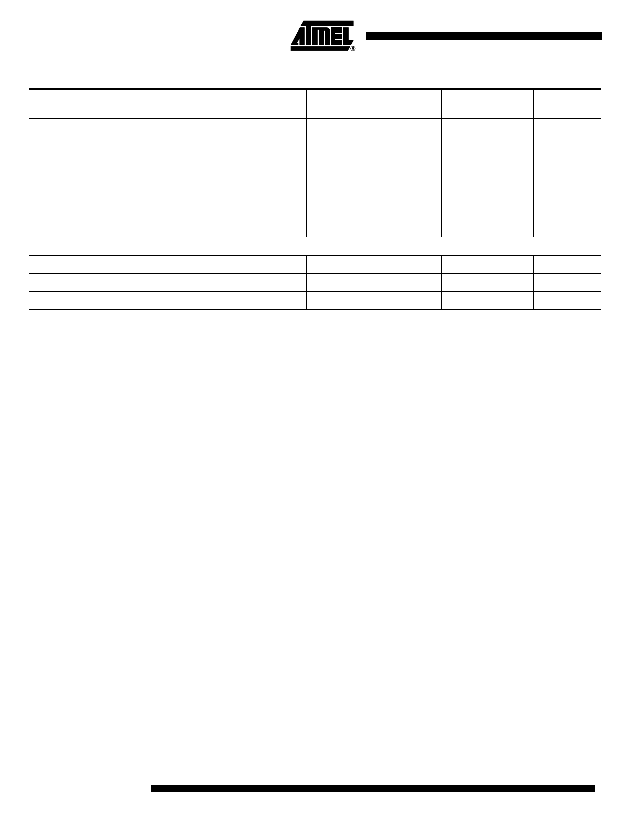
Table 1. PC8240 Pinout Listing (Continued)
Signal Name
Package Pin Number
Pin Type
Power
Supply
Output Driver
Type
Notes
AVdd
C17
Power for
AVdd
–
–
PLL (CPU
Core Logic)
2.5V
AVdd2
AF24
Power for
AVdd2
–
–
PLL
(Peripheral
Logic) 2.5V
Manufacturing Pins
DA2
C25
I/O
OVdd
DRV_PCI
(2)
DA[11 – 13]
AD26 AF17 AF19
I/O
OVdd
DRV_PCI
(2)(6)
DA[14 – 15]
F1 J2
I/O
GVdd
DRV_MEM_ADDR
(2)(6)
Notes: 1. Place pull-up resistors of 120Ω or less on the TEST[0 – 1] pins.
2. Treat these pins as No Connects unless using debug address functionality.
3. This pin has an internal pull-up resistor which is enabled only when the PC8240 is in the reset state. The value of the inter-
nal pull-up resistor is not guaranteed, but is sufficient to ensure that a "1" is read into configuration bits during reset.
4. This pin is a reset configuration pin.
5. DL[0] is a reset configuration pin and has an internal pull-up resistor which is enabled only when the PC8240 is in the reset
state. The value of the internal pull-up resistor is not guaranteed, but is sufficient to insure that a "1" is read into configuration
bits during reset.
6. Multi-pin signals such as AD[0 – 31] or DL[0 – 31] have their physical package pin numbers listed in order corresponding to
the signal names. Ex: AD0 is on pin C22, AD1 is on pin D22,... AD31 is on pin V25.
7. GNT4 is a reset configuration pin and has an internal pull-up resistor which is enabled only when the PC8240 is in the reset
state. The value of the internal pull-up resistor is not guaranteed, but is sufficient to insure that a "1" is read into configuration
bits during reset.
8. Recommend a weak pull-up resistor (2 kΩ – 10 kΩ) be placed on this PCI control pin to LVdd.
9. VIH and VIL for these signals are the same as the PCI VIH and VIL entries in Table 6, “DC Electrical Specifications,” on
page 16.
10. Recommend a weak pull-up resistor (2 kΩ – 10 kΩ) be placed on this pin to OVdd.
11. Recommend a weak pull-up resistor (2 kΩ – 10 kΩ) be placed on this pin to GVdd.
12. This pin has an internal pull-up resistor; the value of the internal pull-up resistor is not guaranteed, but is sufficient to prevent
unused inputs from floating.
13. Output Valid specifications for this pin are memory interface mode dependent (Registered or Flow-through), see Table 11,
“Output AC Timing Specifications,” on page 22.
14. Non-DRAM Access Output Valid specification applies to this pin during non-DRAM accesses, see specification 12b3 in
Table 11, “Output AC Timing Specifications,” on page 22.
15. This pin is affected by programmable PCI_HOLD_DEL parameter, see “PCI Signal Output Hold Timing” on page 23.
16. This pin is an open drain signal.
17. This pin can be programmed to be driven (default) or can be programmed to be open drain; see PMCR2 register description
in the Motorola PC8240 User’s Manual for details.
18. This pin is a Sustained Tri-State pin as defined by the PCI Local Bus Specification.
6 PC8240
2149A–HIREL–05/02
Share Link: 