AT89C2051-12SA View Datasheet(PDF) - Atmel Corporation
Part Name
Description
Manufacturer
AT89C2051-12SA Datasheet PDF : 13 Pages
| |||
AT89C2051
Absolute Maximum Ratings*
Operating Temperature ................................. -55°C to +125°C
Storage Temperature ..................................... -65°C to +150°C
Voltage on Any Pin
with Respect to Ground .....................................-1.0V to +7.0V
Maximum Operating Voltage............................................. 6.6V
DC Output Current...................................................... 25.0 mA
*NOTICE:
Stresses beyond those listed under “Absolute
Maximum Ratings” may cause permanent dam-
age to the device. This is a stress rating only and
functional operation of the device at these or any
other conditions beyond those indicated in the
operational sections of this specification is not
implied. Exposure to absolute maximum rating
conditions for extended periods may affect device
reliability.
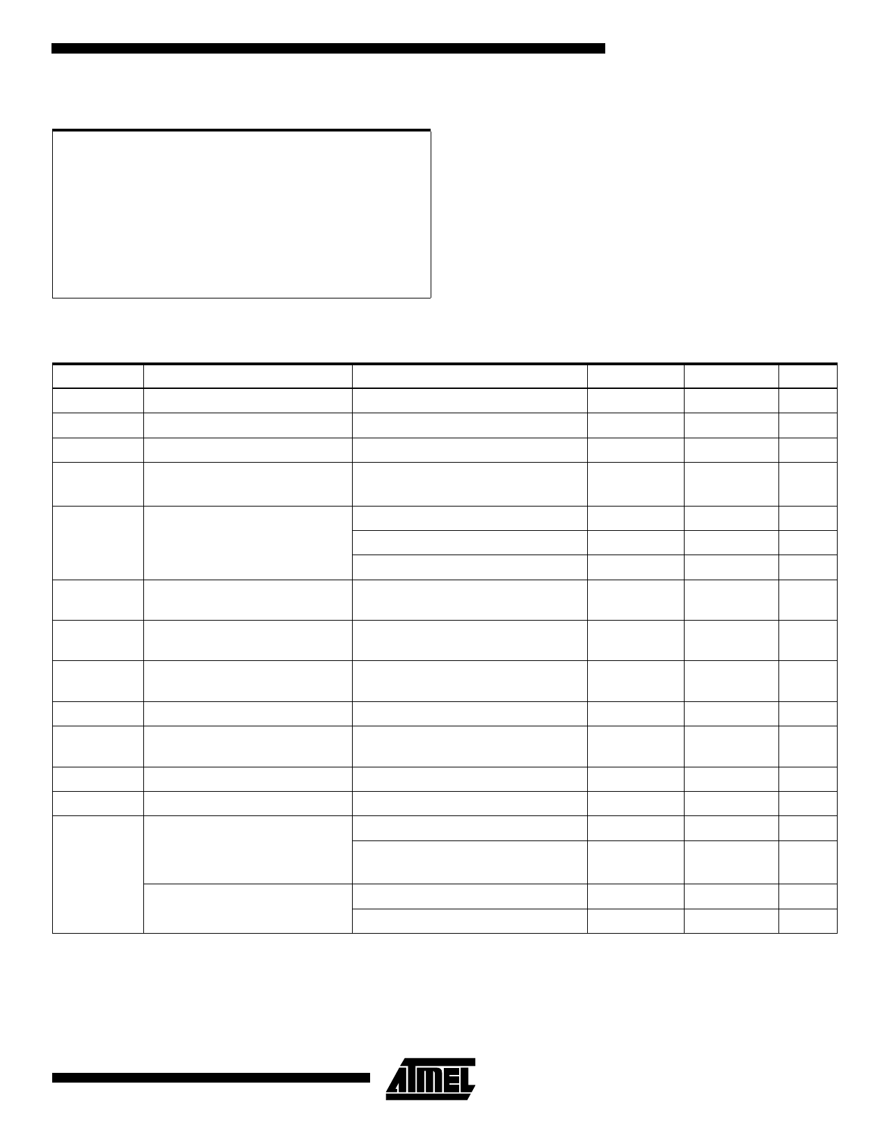
DC Characteristics
TA = -40°C to 85°C, VCC = 2.0V to 6.0V (unless otherwise noted)
Symbol
Parameter
Condition
Min
Max
Units
VIL
Input Low Voltage
VIH
Input High Voltage
VIH1
Input High Voltage
VOL
Output Low Voltage(1)
(Ports 1, 3)
(Except XTAL1, RST)
(XTAL1, RST)
IOL = 20 mA, VCC = 5V
IOL = 10 mA, VCC = 2.7V
-0.5
0.2 VCC - 0.1
V
0.2 VCC + 0.9 VCC + 0.5
V
0.7 VCC
VCC + 0.5
V
0.5
V
VOH
Output High Voltage
(Ports 1, 3)
IIL
Logical 0 Input Current
(Ports 1, 3)
IOH = -80 µA, VCC = 5V ± 10%
IOH = -30 µA
IOH = -12 µA
VIN = 0.45V
2.4
V
0.75 VCC
V
0.9 VCC
V
-50
µA
ITL
Logical 1 to 0 Transition Current VIN = 2V, VCC = 5V ± 10%
(Ports 1, 3)
-750
µA
ILI
Input Leakage Current
0 < VIN < VCC
(Port P1.0, P1.1)
±10
µA
VOS
Comparator Input Offset Voltage VCC = 5V
VCM
Comparator Input Common
Mode Voltage
20
mV
0
VCC
V
RRST
Reset Pulldown Resistor
50
300
KΩ
CIO
ICC
Notes:
Pin Capacitance
Test Freq. = 1 MHz, TA = 25°C
10
pF
Power Supply Current
Active Mode, 12 MHz, VCC = 6V/3V
15/5.5
mA
Power Down Mode(2)
Idle Mode, 12 MHz, VCC = 6V/3V
P1.0 & P1.1 = 0V or VCC
VCC = 6V P1.0 & P1.1 = 0V or VCC
5/1
mA
100
µA
VCC = 3V P1.0 & P1.1 = 0V or VCC
20
µA
1. Under steady state (non-transient) conditions, IOL must be externally limited as follows:
Maximum IOL per port pin: 20 mA
Maximum total IOL for all output pins: 80 mA
If IOL exceeds the test condition, VOL may exceed the related specification. Pins are not guaranteed to sink current greater
than the listed test conditions.
2. Minimum VCC for Power Down is 2V.
4-23
Share Link: 