LC868364A View Datasheet(PDF) - SANYO -> Panasonic
Part Name
Description
Manufacturer
LC868364A
SANYO -> Panasonic

LC868364A Datasheet PDF : 29 Pages
| |||
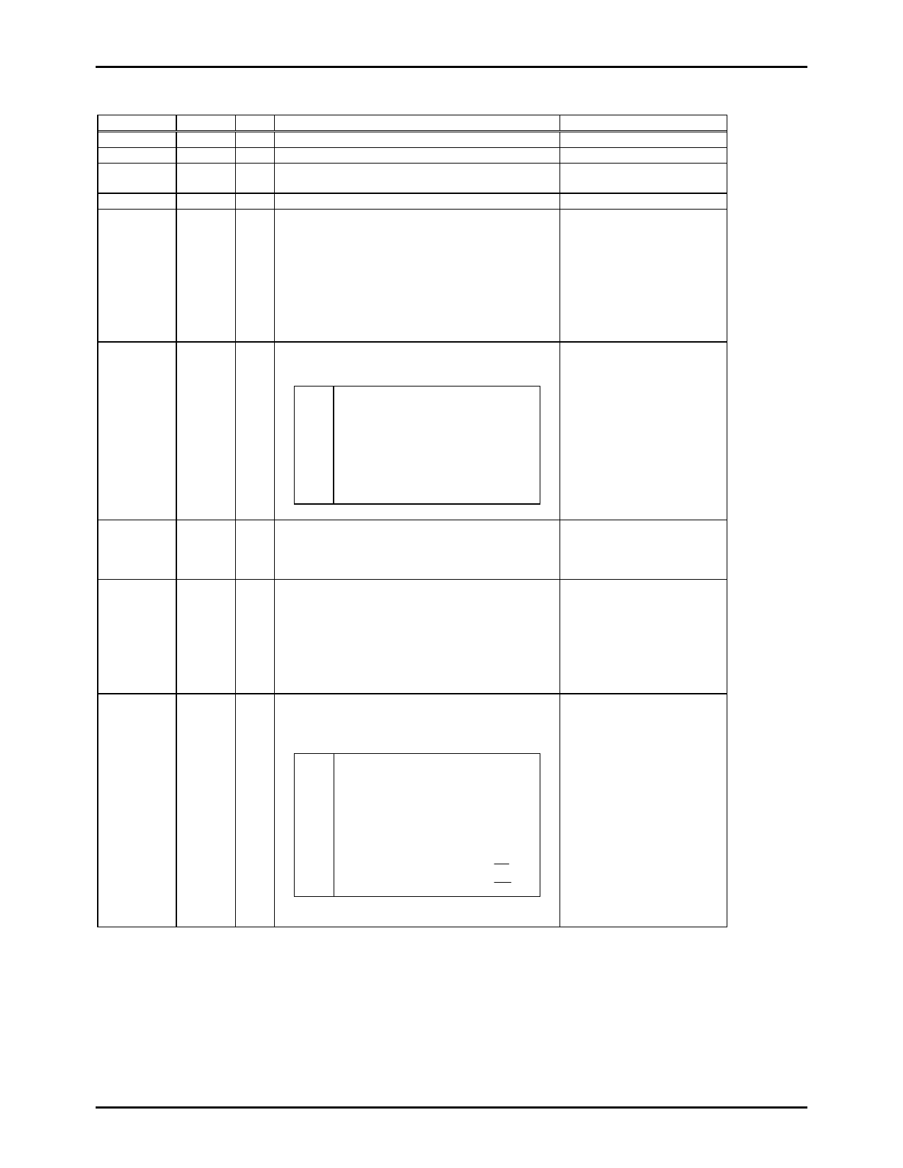
Pad Description
LC868364A
Name
VSS
VDD
VLCD
V1 to V5
Port0
P00 to P07
Port1
P10 to P17
Port2
P20 to P27
Port3
P30 to P37
Port4
P40 to P47
No. I/O
Function Description
74,133 - Power terminal (-)
1,103
- Power terminal (+)
4
- Power terminal (+) for LCD driver
(for bleeder resistor)
9-5
- Voltage supply terminals to LCD drivers
I/O ! 8-bit input/output port
! Data direction programmable in nibble units
112-119
! External memory mode
1. EXT register bit 2=0
Address output of lower 8 bits, input/output
of data
87-94
2. EXT register bit 2=1
! Input/output of data
! Input for key interrupt (P30INT=0) (Note 2)
I/O ! 8-bit input/output port
! Data direction programmable for each bit individually
! Other functions
P10 SIO0 data output
P11 SIO0 data input, bus input/output
P12 SIO0 clock input/output
P13 SIO1 data output
P14 SIO1 data input, bus input/output
P15 SIO1 clock input/output
P16 Buzzer output
P17 Timer 1 output (PWM output)
Option
-
-
-
-
! Pull-up resistor:
provided/not provided
! Output form:
CMOS/N-ch open drain
(Note 1)
! Output form:
CMOS/N-ch open drain
(Note 1)
120-127
104-111
75-82
I/O ! 8-bit input/output port
! Input/output can be specified in a bit
! External memory mode
! Output form:
CMOS/N-ch open drain
(Note 1)
Address output of upper 8 bits
I/O ! 8-bit input/output port
! Data direction programmable for each bit individually
! External memory mode
1. EXT register bit 2=0: input/output port
! Pull-up resistor:
provided/not provided
! Output form:
CMOS/N-ch open drain
2. EXT register bit 2=1:
address output of lower 8
(Note 1)
bits for external memory
! Input for key interrupt (P30INT=L) (Note 2)
I/O ! 8-bit input/output port
! Input/output can be specified each upper
2 bits and lower 6 bits
! Other functions
! Pull-up resistor:
provided/not provided
! Output form:
CMOS/N-ch open drain
P40 Externally boosted clock 2KOUT
(Note 1)
P41 Shift clock
CL2
P42 System clock for expansion
driver
LCDP2
P43 Alternate signal
M
P44 General output port
P44
P45 General output port
P45
P46 Read signal
RD
P47 Write signal
WR
(P40-P43: LCD expansion signal,
P46, P47: External RAM access signal)
No.6722-11/29
Share Link: