PIC16F688 View Datasheet(PDF) - Microchip Technology
Part Name
Description
Manufacturer
PIC16F688
Microchip Technology

PIC16F688 Datasheet PDF : 202 Pages
| |||
PIC16F688
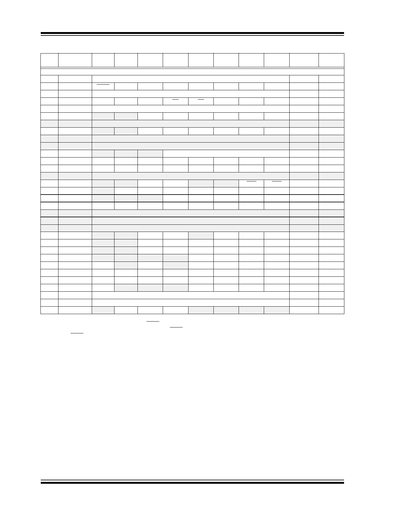
TABLE 2-2: PIC16F688 SPECIAL FUNCTION REGISTERS SUMMARY BANK 1
Addr
Name
Bit 7
Bit 6
Bit 5
Bit 4
Bit 3
Bit 2
Bit 1
Bit 0
Value on
POR/BOR
Page
Bank 1
80h INDF
Addressing this location uses contents of FSR to address data memory (not a physical register) xxxx xxxx 20, 117
81h OPTION_REG RAPU INTEDG T0CS
T0SE
PSA
PS2
PS1
PS0 1111 1111 14, 117
82h PCL
Program Counter’s (PC) Least Significant Byte
0000 0000 19, 117
83h STATUS
IRP
RP1
RP0
TO
PD
Z
DC
C
0001 1xxx 13, 117
84h FSR
Indirect Data Memory Address Pointer
xxxx xxxx 20, 117
85h TRISA
—
—
TRISA5 TRISA4 TRISA3 TRISA2 TRISA1 TRISA0 --11 1111 33, 117
86h
—
Unimplemented
—
—
87h TRISC
—
—
TRISC5 TRISC4 TRISC3 TRISC2 TRISC1 TRISC0 --11 1111 42, 117
88h
—
Unimplemented
—
—
89h
—
Unimplemented
—
—
8Ah PCLATH
8Bh INTCON
—
—
—
Write Buffer for upper 5 bits of Program Counter
---0 0000 19, 117
GIE
PEIE
T0IE
INTE
RAIE
T0IF
INTF
RAIF(3) 0000 000x 15, 117
8Ch PIE1
EEIE
ADIE
RCIE
C2IE
C1IE
OSFIE
TXIE
TMR1IE 0000 0000 16, 117
8Dh
—
Unimplemented
—
—
8Eh PCON
—
—
ULPWUE SBOREN
—
—
POR
BOR --01 --qq 18, 117
8Fh OSCCON
—
IRCF2 IRCF1
IRCF0
OSTS
HTS
LTS
SCS -110 x000 22, 118
90h OSCTUNE
—
—
—
TUN4
TUN3
TUN2
TUN1
TUN0 ---0 0000 26, 118
91h ANSEL
ANS7 ANS6
ANS5
ANS4
ANS3
ANS2
ANS1
ANS0 1111 1111 34, 118
92h
—
Unimplemented
—
—
93h
—
Unimplemented
—
—
94h
—
Unimplemented
—
—
95h WPUA(2)
—
—
WPUA5 WPUA4
—
WPUA2 WPUA1 WPUA0 --11 -111 35, 118
96h IOCA
—
—
IOCA5
IOCA4
IOCA3
IOCA2
IOCA1
IOCA0 --00 0000 35, 118
97h EEDATH
—
—
EEDATH5 EEDATH4 EEDATH3 EEDATH2 EEDATH1 EEDATH0 --00 0000 78, 118
98h EEADRH
—
—
—
—
EEADRH3 EEADRH2 EEADRH1 EEADRH0 ---- 0000 78, 118
99h VRCON
VREN
—
VRR
—
VR3
VR2
VR1
VR0 0-0- 0000 63, 118
9Ah EEDAT
EEDAT7 EEDAT6 EEDAT5 EEDAT4 EEDAT3 EEDAT2 EEDAT1 EEDAT0 0000 0000 78, 118
9Bh EEADR
EEADR7 EEADR6 EEADR5 EEADR4 EEADR3 EEADR2 EEADR1 EEADR0 0000 0000 78, 118
9Ch EECON1
EEPGD
—
—
—
WRERR WREN
WR
RD
x--- x000 79, 118
9Dh EECON2
EEPROM Control 2 Register (not a physical register)
---- ---- 77, 118
9Eh ADRESL
Least Significant 2 bits of the left shifted result or 8 bits of the right shifted result
xxxx xxxx 72, 118
9Fh ADCON1
—
ADCS2 ADCS1 ADCS0
—
—
—
—
-000 ---- 71, 118
Legend:
Note 1:
2:
3:
– = Unimplemented locations read as ‘0’, u = unchanged, x = unknown, q = value depends on condition, shaded = unimplemented
Other (non Power-up) Resets include MCLR Reset and Watchdog Timer Reset during normal operation.
RA3 pull-up is enabled when pin is configured as MCLR in the Configuration Word register.
MCLR and WDT Reset does not affect the previous value data latch. The RAIF bit will be cleared upon Reset but will set again if the
mismatched exists.
DS41203D-page 10
© 2007 Microchip Technology Inc.
Share Link: